

Page 1
Any and all SANYO products described or contained herein do not have specifications that can handle
applications that require extremely high levels of reliability, such as life-support systems, aircraft’s
control systems, or other applications whose failure can be reasonably expected to result in serious
physical and/or material damage. Consult with your SANYO representative nearest you before using
any SANYO products described or contained herein in such applications.
SANYO assumes no responsibility for equipment failures that result from using products at values that
exceed, even momentarily, rated values (such as maximum ratings, operating condition ranges,or other
parameters) listed in products specifications of any and all SANYO products described or contained
herein.
Monolithic Linear IC
Multifunction Multiple Voltage Regulator
Ordering number:ENN2301B
LA5665
SANYO Electric Co.,Ltd. Semiconductor Company
TOKYO OFFICE Tokyo Bldg., 1-10, 1 Chome, Ueno, T aito-ku, TOKYO, 110-8534 JAPAN
18.0
3.0
Overview
• Especially suited for use in micorcomputer-controlled
tuners, receivers, preamplifiers and the like.
Features
• Two independent voltage regulators contained in a single
chip (15.5V/350mA, 5.6V/100mA).
• Reset circuit which delivers the reset signal on the positive transition, negative transition of the 5.6V output.
• Muting circuit which detects the 15.5V output and reset
output to deliver the muting signal (We have the LA5666
whose detection function for reset, muting is provided on
the input voltage side).
Specifications
Maximum Ratings at Ta = 25˚C
retemaraPlobmySsnoitidnoCsgnitaRtinU
egatlovtupnIV
tnerructuptuOI
noitapissidrewopelbawollAxamdPylnoCI 6.1W
erutarepmetgnitarepOrpoT 08+ot03–
erutarepmetegarotSgtsT 521+ot04–
2,1 53V
NI
2,1lanretnI
TUO
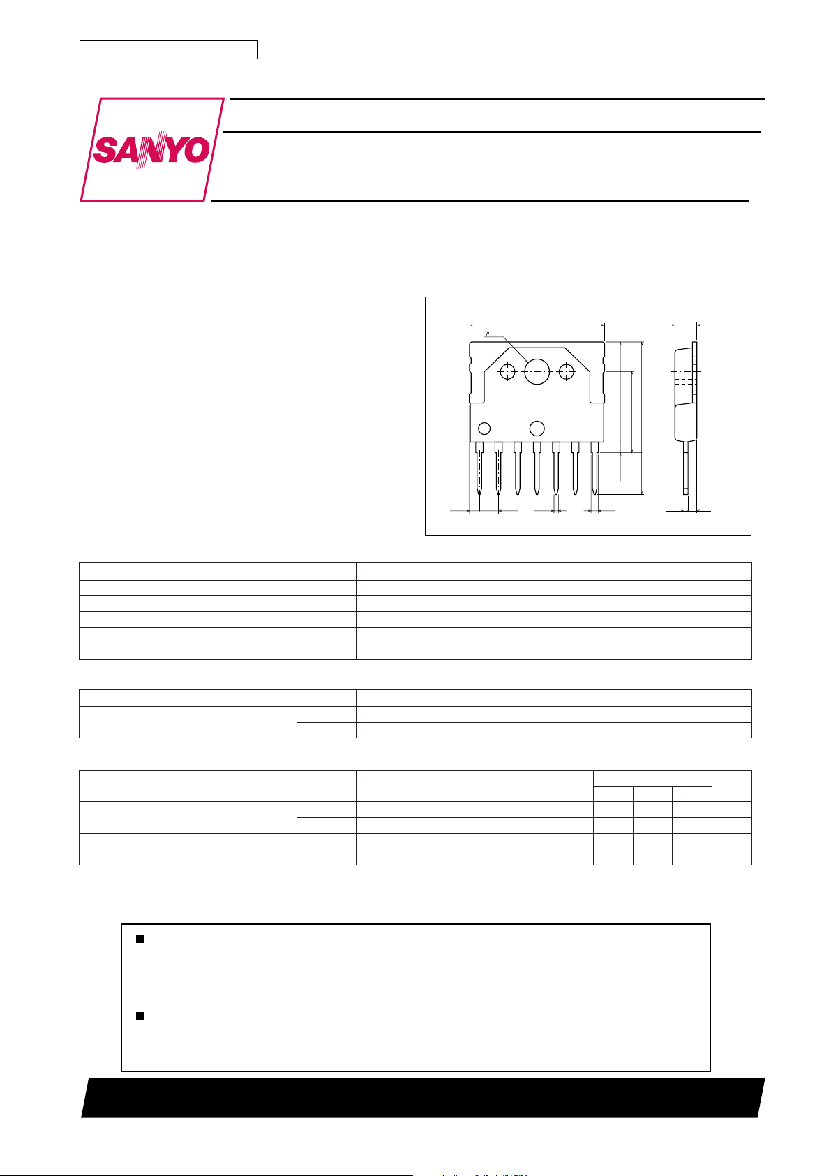
Package Dimensions
unit:mm
3075-SIP7H
[LA5665]
3.4
1.38
1
2.54
0.6
7
13.4
10.8
15.0max
5.8
1.0min
1.0
0.6 1.2
SANYO : SIP7H
˚C
˚C
Operating Conditions at Ta = 25˚C
retemaraPlobmySsnoitidnoCsgnitaRtinU
egatlovtupnI
VNI1I
VNI2I
Am002=1 53ot91V
TUO
Am05=2 53ot7.8V
TUO
Operating Characteristics at Ta = 25˚C, VIN1=20V, VIN2=10V
retemaraPlobmySsnoitidnoC
INI18.18.28.3Am
INI28.38.58.7Am
VO1I
VO2I
Am002=15.415.515.61V
TUO
Am05=21.56.52.6V
TUO
tnerructnecseiuQ
egatlovtuptuO
40500TN (KT)/83094HK/8287KI/7256KI, TS No.2301–1/4
sgnitaR
nimpytxam
Continued on next page.
tinU
Page 2
LA5665
Continued from preceding page.
retemaraPlobmySsnoitidnoC
noitalugereniL
noitalugerdaoL
noitcejerelppiR
pordegatlovtuptuo-tupnI
egatlovtcetedteseRV
egatloverapmocremiT
tnerrucsaibtupniremiTI
egatlovtcetedgnituMV
egatlovtuptuognituMV
Vlo1V
Vlo2V
V
V
R
VC10.12.14.1V
VC260.031.081.0V
M
NI
NI
1I
dlo
O
2I
dlo
O
1rRI,zH021=f
2rRI,zH021=f
1rdVIOAm002=6.15.2V
2rdVIOAm05=5.15.2V
BT
I
ETUMO
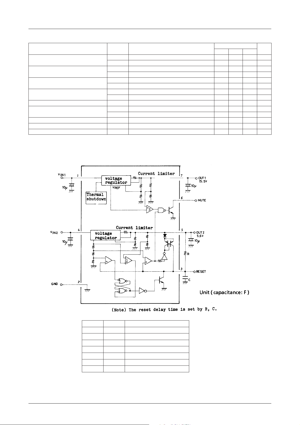
Note 1 : VR is the voltage of VO2 at the time reset is turned OFF.
Note 2 : VM is the voltage of VO1 at the time muting is turned OFF.
Equivalent Circuit Block Diagram, Pin Assignment, and Peripheral Circuit
V72ot91=2602Vm
V81ot9=2202Vm
Am053ot0=0103Vm
Am001ot0=202Vm
Am002=6556Bd
O
Am05=0657Bd
O
)1etoN(9.41.55.5V
)2etoN(5.315.415.51V
Am5=1.051.0V
ETUMO
sgnitaR
nimpytxam
tinU
052An
.oNniPemaNnoitpircseD
1V
2DNGdnuorG
3TESERniptuptuodnaemityaledteseR
4V
52TUOniptuptuoV6.5
6ETUMniptuptuolangisgnituM
71TUOniptuptuoV5.51
1eniltuptuoV5.51rofniptupnI
NI
2eniltuptuoV6.5rofniptupnI
NI
No.2301–2/4
Page 3

Operating Waveforms
LA5665
No.2301–3/4
Page 4

LA5665
Specifications of any and all SANYO products described or contained herein stipulate the performance,
characteristics, and functions of the described products in the independent state, and are not guarantees
of the performance, characteristics, and functions of the described products as mounted in the customer's
products or equipment. To verify symptoms and states that cannot be evaluated in an independent device,
the customer should always evaluate and test devices mounted in the customer's products or equipment.
SANYO Electric Co., Ltd. strives to supply high-quality high-reliability products. However, any and all
semiconductor products fail with some probability. It is possible that these probabilistic failures could
give rise to accidents or events that could endanger human lives, that could give rise to smoke or fire,
or that could cause damage to other property. When designing equipment, adopt safety measures so
that these kinds of accidents or events cannot occur. Such measures include but are not limited to protective
circuits and error prevention circuits for safe design, redundant design, and structural design.
In the event that any or all SANYO products(including technical data,services) described or
contained herein are controlled under any of applicable local export control laws and regulations,
such products must not be exported without obtaining the export license from the authorities
concerned in accordance with the above law.
No part of this publication may be reproduced or transmitted in any form or by any means, electronic or
mechanical, including photocopying and recording, or any information storage or retrieval system,
or otherwise, without the prior written permission of SANYO Electric Co. , Ltd.
Any and all information described or contained herein are subject to change without notice due to
product/technology improvement, etc. When designing equipment, refer to the "Delivery Specification"
for the SANYO product that you intend to use.
Information (including circuit diagrams and circuit parameters) herein is for example only ; it is not
guaranteed for volume production. SANYO believes information herein is accurate and reliable, but
no guarantees are made or implied regarding its use or any infringements of intellectual property rights
or other rights of third parties.
This catalog provides information as of April, 2000. Specifications and information herein are subject to
change without notice.
PS No.2301–4/4
 Loading...