

Page 1
Ordering number : ENN5998
22500RM (OT) No. 5998-1/6
Overview
The LA5632 is a multiple power supply IC that provides
two 3.3-V regulator circuits as well as two 5-V regulator
circuits. This device is optimal for MD players and similar
applications.
Functions and Features
• Two built-in 3.3-V regulator circuits (IO= 60 mA,
150 mA)
• Two built-in 5-V regulator circuits (IO= 1000 mA,
100 mA)
• Power on/off detection circuit included
• The reset circuit operates from the B.BAK voltage.
• The reset circuit current drain is extremely low (3.5 µA
(typical) in backup mode)
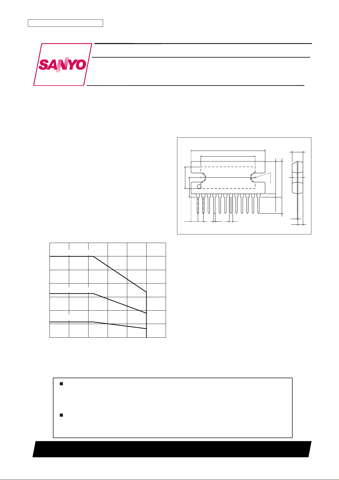
Package Dimensions
unit: mm
3149A-SIP12H
27.0
20.0
R1.7
8.4
121
11.8
0.5
2.0
4.0
0.4
2.0
7.0
2.5
1.0
13.2max
6.0
1.0min
0–20 20 40 60 80 100
2
2.3
4
6
6.5
8
10
12
14
0
Pd max — Ta
100 × 100 × 1.5 mm
3
50 × 50 × 1.5 mm
3
1.3
3.6
6.7
SANYO: SIP12H
[LC5632]
LA5632
SANYO Electric Co.,Ltd. Semiconductor Company
TOKYO OFFICE Tokyo Bldg., 1-10, 1 Chome, Ueno, Taito-ku, TOKYO, 110-8534 JAPAN
Multiple Power Supply System Regulator
Monolithic linear IC
Any and all SANYO products described or contained herein do not have specifications that can handle
applications that require extremely high levels of reliability, such as life-support systems, aircraft’s
control systems, or other applications whose failure can be reasonably expected to result in serious
physical and/or material damage. Consult with your SANYO representative nearest you before using
any SANYO products described or contained herein in such applications.
SANYO assumes no responsibility for equipment failures that result from using products at values that
exceed, even momentarily, rated values (such as maximum ratings, operating condition ranges, or other
parameters) listed in products specifications of any and all SANYO products described or contained
herein.
Ambient temperature, Ta — °C
Allowable power dissipation, Pd max — mW
Independent IC
Page 2
No. 5998-2/6
LA5632
Parameter Symbol Conditions Ratings Unit
Input voltage V
CC
max 14 V
AC input voltage AC max 2V
Allowable power dissipation Pd max Independent IC 2.3 W
Operating temperature Topr –20 to +80 °C
Storage temperature Tstg –55 to +150 °C
Specifications
Maximum Ratings at Ta = 25°C
Parameter Symbol Conditions Ratings Unit
Input voltage V
CC
6.25 to 12 V
Reset circuit input voltage V
B.BAK
1.4 to 3.5 V
PH5 output current I
PH5
0 to 1000 mA
B.BAK output current I
B.BAK
0 to 60 mA
ANA5 output current I
ANA5
0 to 100 mA
SYS3.3 output current I
SYS3.3
0 to 150 mA
S.RESET sink current I
SINKS
0 to 0.2 mA
P.DOWN sink current I
SINKP
0 to 1 mA
AC input current I
AC
0 to 1 mA
Operating Conditions at Ta = 25°C
Parameter Symbol Conditions
Ratings
Unit
min typ max
[PH5 Regulator Block] V
CC
= 10 V, I
PH5
= 1000 mA
Output voltage V
O
PH5 4.75 5 5.25 V
Dropout voltage V
DROP
PH5 0.5 1 V
Line regulation ∆V
OLN
PH5 VCC= 6.25 to 12 V 200 mV
Load regulation ∆V
OLD
PH5 I
PH5
= 5 to 1000 mA 200 mV
Peak output current I
OP
PH5 1000 1400 mA
Output shorted current I
OSC
PH5 400 1000 mA
Current drain I
Q
PH5 70 112 mA
[SYS3.3 Regulator Block] V
CC
= 10 V, I
SYS3.3
= 150 mA
Output voltage V
O
SYS3.3 3.13 3.3 3.47 V
Dropout voltage V
DROP
SYS3.3 2 3.5 V
Line regulation ∆V
OLN
SYS3.3 VCC= 6.25 to 12 V 200 mV
Load regulation ∆V
OLD
SYS3.3 I
SYS3.3
= 5 to 150 mA 200 mV
Peak output current I
OP
SYS3.3 150 210 mA
Output shorted current I
OSC
SYS3.3 200 450 mA
Current drain I
Q
SYS3.3 17.5 28 mA
[ANA5 Regulator Block] V
CC
= 10 V, I
ANA5
= 1000 mA
Output voltage V
O
ANA5 4.75 5 5.25 V
Dropout voltage V
DROP
ANA5 0.5 1 V
Line regulation ∆V
OLN
ANA5 VCC= 6.25 to 12 V 200 mV
Load regulation ∆V
OLD
ANA5 I
ANA5
= 5 to 100 mA 200 mV
Peak output current I
OP
ANA5 100 140 mA
Output shorted current I
OSC
ANA5 40 100 mA
Current drain I
Q
ANA5 17.5 28 mA
Output noise voltage V
NO
ANA 10 Hz ≤ f ≤ 100 kHz 120 µV
Electrical Characteristics at Ta = 25°C
Continued on next page.
Page 3

No. 5998-3/6
LA5632
Parameter Symbol Conditions
Ratings
Unit
min typ max
[B.BAK Regulator Block] V
CC
= 10 V, I
BAK
= 60 mA
Output voltage V
O
BAK 3.13 3.3 3.47 V
Dropout voltage V
DROP
BAK 2 2.5 V
Line regulation ∆V
OLN
BAK VCC= 6.25 to 12 V 200 mV
Load regulation ∆V
OLD
BAK I
BAK
= 5 to 60 mA 200 mV
Peak output current I
OP
BAK 60 84 mA
Output shorted current I
OSC
BAK 60 180 mA
Current drain I
Q
BAK 15 24 mA
[P.DOWN Detection Circuit] V
CC
= 10 V
Threshold voltage V
TH
P.DOWN 3.0 3.16 3.32 V
Residual voltage Vsat P.DOWN
With the cd1 pin shorted
200 mV
P.DOWN pin current = 1 mA
Delay time td1 cd1 = 1 µF 75 100 125 ms
[S.RESET Block] V
CC
= 0 V, B.BAK = 3.3 V
Threshold voltage1 V
TH
1 S.RESET 2.56 2.7 2.84 V
Threshold voltage2 V
TH
2 S.RESET 1.9 2.0 2.1 V
Reset output undefined voltage V
UNS
S.RESET 1.4
Backup mode current drain I
IN
1 BAK B.BAK = 3.1 V 3.5 5 µA
Low-level output current drain I
IN
2 BAK B.BAK = 1.8 V 0.36 mA
Residual voltage Vsat S.RESET
With the cd2 pin shorted
200 mV
S.RESET pin current = 0.2 mA
Delay time td2 cd2 = 1 µF 75 100 125 ms
[AC Detection Circuit] V
CC
= 10 V
Threshold voltage V
TH
AC 0.5 0.7 0.9 V
[STBY Detection Circuit] V
CC
= 10 V
Threshold voltage V
TH
STBY 1.3 1.8 2.3 V
Continued from preceding page.
Page 4

Pin Assignment
No. 5998-4/6
LA5632
1
PH5
2
STBY
3
V
CC
4
ANA5
5
SYS3.3
6
B.BAK
7AC8
CD1
9
P.DOWN
10
GND
11
CD2
12
S.RESET
LA5632
A11324
Block Diagram
To the microcontroller
Note: Use capacitors with low capacitance temperature coefficients for all capacitors.
3
V
CC
9
P.DOWN
8
CD1
2
STBY
7
AC
12
S.RESET
1
PH5
6
B.BAK
4
ANA5
5
SYS3.3
10
GND
10 kΩ
1000 pF
1 µF
100 µF
11
CD2
1 µF
100 kΩ
1000 pF
B.BAK
22 kΩ
1 kΩ
1 kΩ
10 µF
100 Ω
100 µF
100 µF
100 µF
10 µF
3.3 V
V
REF
A11325
Delay circuit
Microcontroller
To SYS3.3
Delay circuit
To the microcontroller
Page 5

Timing Chart
No. 5998-5/6
LA5632
0
0
0
0
0
0
0
0
0
Vuns S.RESET
VTH P.DOWN
VTH1 S.RESET
VTH2 S.RESET
Vuns S.RESET
VTH AC
Td2
Td1
A11326
P.DOWN
S.RESET
AC pin
Note: The S.RESET output has an undefined operating state, so care is required in application design.
VCC pin
ANA output
B.BAK pin
Backup
PH5 pin
SYS3.3 output
Operation undefined
Operation undefined
Page 6

PS No. 5998-6/6
LA5632
This catalog provides information as of February, 2000. Specifications and information herein are subject
to change without notice.
Specifications of any and all SANYO products described or contained herein stipulate the performance,
characteristics, and functions of the described products in the independent state, and are not guarantees
of the performance, characteristics, and functions of the described products as mounted in the customer’s
products or equipment. To verify symptoms and states that cannot be evaluated in an independent device,
the customer should always evaluate and test devices mounted in the customer’s products or equipment.
SANYO Electric Co., Ltd. strives to supply high-quality high-reliability products. However, any and all
semiconductor products fail with some probability. It is possible that these probabilistic failures could
give rise to accidents or events that could endanger human lives, that could give rise to smoke or fire,
or that could cause damage to other property. When designing equipment, adopt safety measures so
that these kinds of accidents or events cannot occur. Such measures include but are not limited to protective
circuits and error prevention circuits for safe design, redundant design, and structural design.
In the event that any or all SANYO products (including technical data, services) described or contained
herein are controlled under any of applicable local export control laws and regulations, such products must
not be exported without obtaining the export license from the authorities concerned in accordance with the
above law.
No part of this publication may be reproduced or transmitted in any form or by any means, electronic or
mechanical, including photocopying and recording, or any information storage or retrieval system,
or otherwise, without the prior written permission of SANYO Electric Co., Ltd.
Any and all information described or contained herein are subject to change without notice due to
product/technology improvement, etc. When designing equipment, refer to the “Delivery Specification”
for the SANYO product that you intend to use.
Information (including circuit diagrams and circuit parameters) herein is for example only; it is not
guaranteed for volume production. SANYO believes information herein is accurate and reliable, but
no guarantees are made or implied regarding its use or any infringements of intellectual property rights
or other rights of third parties.
 Loading...