

SANYO LA5623M Datasheet
Parameter Symbol Conditions Ratings Unit
Supply voltage V
CC
–0.3 to +12 V
Output 1 sink current I
SINK
1 8mA
Output 2 sink current I
SINK
2 8mA
Output voltage V
O
–0.3 to +10 V
Manual input voltage V
RES
–0.3 to +10 V
Input voltage range V
IN
1 –0.3 to +10 V
Ct0, Ct1 voltage Vct 0 to +10 V
Allowable power dissipation Pd max 250 mW
Operating temperature Topr –20 to +75 °C
Storage temperature Tstg –40 to +125 °C
Ordering number : EN5719
63097HA(OT) No. 5719-1/4
Overview
The LA5623M is a combination reset IC that provides two
reset functions. The first, reset 1, detects the input voltage
and applies a reset to the CPU system and other logic
systems. The second, reset 2, detects the power supply
voltage when the power is turned on or off, and applies a
reset to the CPU system and other logic systems. This
latter function allows the reset time to be adjusted from
two external pins.
Features
• Reset circuit (output 1) that detects the input voltage and
provides a delay time of 200 µs.
• System reset circuit (output 2) that provides a switchable
delay time of 25, 50, 100, or 200 ms.
• Low operating limit voltage
• Both reset 1 and reset 2 have hysteresis characteristics.
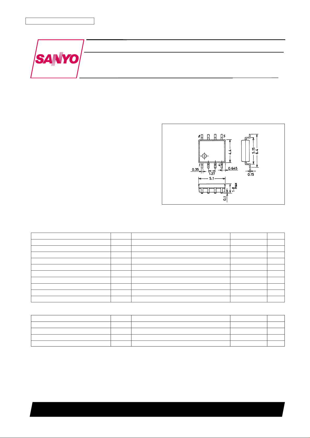
Package Dimensions
unit: mm
3032B-MFP8
SANYO: MFP8
[LA5623M]
LA5623M
SANYO Electric Co.,Ltd. Semiconductor Bussiness Headquarters
TOKYO OFFICE Tokyo Bldg., 1-10, 1 Chome, Ueno, Taito-ku, TOKYO, 110 JAPAN
Monolithic Linear IC
Parameter Symbol Conditions Ratings Unit
Recommended supply voltage V
CC
2 to 10 V
Input voltage range V
IN
For pulse widths of up to 20 ns –2 to VCC+ 1 V
Input high-level voltage V
RESH
For pulse widths of up to 20 ns VCC+ 1 V
Input low-level voltage V
RESL
For pulse widths of up to 20 ns –2 V
Operating Conditions at Ta = 25°C
Specifications
Maximum Ratings at Ta = 25°C
Combination System Reset IC
Parameter Symbol Conditions
Ratings
Unit
min typ max
[Reset Circuit 1, 2 Common]
Current drain when off I
CC
1 – 1.4 2.0 mA
Current drain when on I
CC
2 When reset 1 and 2 are both on – 2 3 mA
Detection voltage temperature coefficient VS/∆T – 0.01 %/°C
Output high-level voltage V
OH
IOH= –40 µA 0.9 V
CC
– – V
Low-level signal propagation delay tPHL C
L
= 100 pF – 10 – µs
Operating limit voltage *1 V
OPL
RL= 2.2 kΩ, V(sat) ≤ 0.4 V – 0.67 0.80 V
R
L
= 100 kΩ, V(sat) ≤ 0.4 V – 0.55 0.70 V
Internal pull-up resistance R 5 10 15 kΩ
[Reset Circuit 1]
Sense voltage 1 VS1 1.20 1.25 1.30 V
Hysteresis voltage 1 ∆VS1 9 15 23 mV
High-level signal propagation delay 1 tPLH1 C
L
= 100 pF 80 200 500 µs
Output low voltage 1 V
OL
1 VIN< 1.2 V, IOL= 5 mA – 0.2 0.4 V
Input voltage range V
IN
1 –0.3 – +10 V
Input current I
IN
1 VIN= 1.25 V – 100 500 nA
[Reset Circuit 2]
Sense voltage 2 VS2 4.0 4.2 4.4 V
Hysteresis voltage 2 ∆VS2 30 50 100 mV
Ct0 = “L”, Ct1 = “H” : CL = 100pF 15 25 35 ms
High-level signal propagation delay 2 tPLH2
Ct0 = “H”, Ct1 = “L” : CL = 100pF 30 50 70 ms
Ct0 = “H”, Ct1 = “H” : CL = 100pF 60 100 140 ms
Ct0 = “L”, Ct1 = “L” : CL = 100pF 120 200 280 ms
Output low-level voltage 2 V
OL
2 VCC< 4.0 V, IOL= 5 mA – 0.2 0.4 V
Input high-level voltage *
2
V
RESH
2 2 – 10 V
Input high-level current *
2
I
RESH
2 V
RES
= 2 V – – 80 µA
Input low-level voltage *
2
V
RESL
2 –0.3 – +0.8 V
No. 5719-2/4
LA5623M
Notes: 1. The minimum supply voltage such that a low-level output can be maintained.
2. Manual reset.
A high level applied to the manual reset pin sets the output 2 pin low, and a low level sets the output 2 pin high.
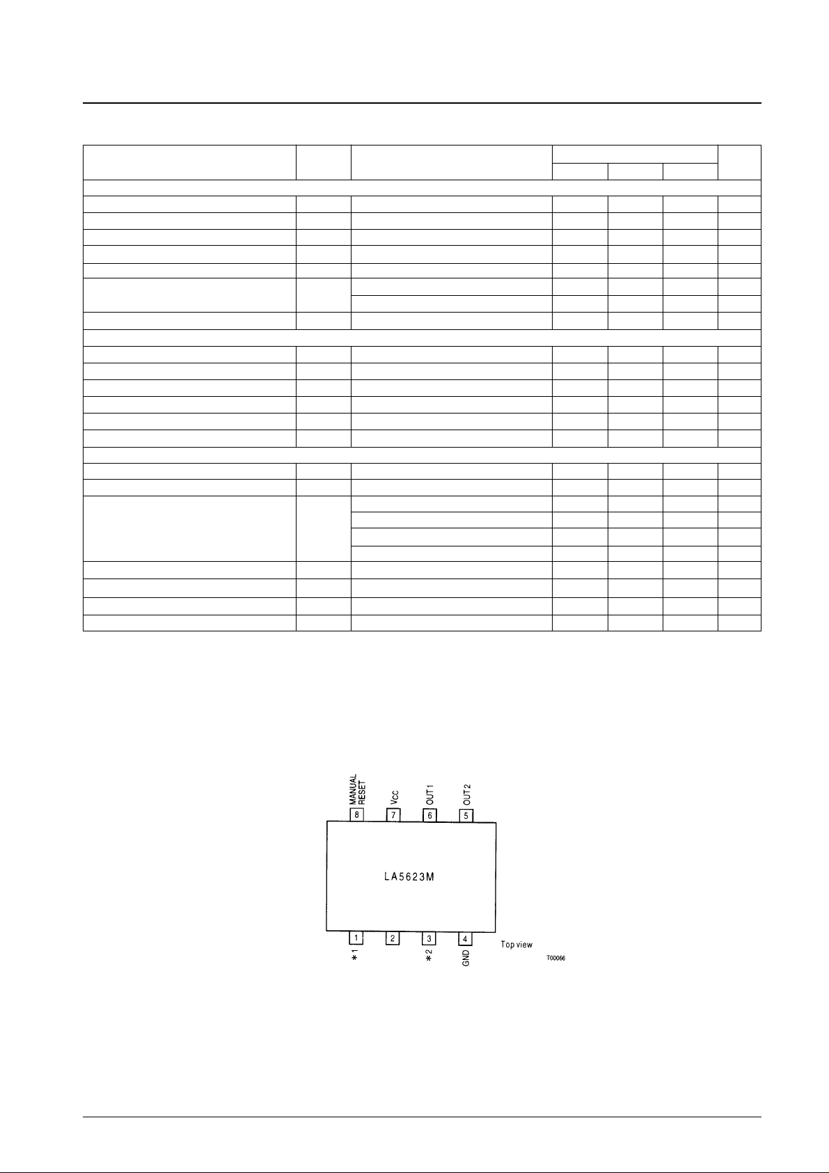
Pin Assignment
*1: Ct0
*2: Ct1
The delay time is 100 ms when
the above two pins are both
left open.
INPUT
Operating Characteristics at Ta = 25°C, VCC= 5 V
 Loading...