

SANYO LA5620 Datasheet
Regulator for Multiple Power Supply Systems
Parameter Symbol Conditions Ratings Unit
Input voltage V
CC
max 14 V
AC input voltage AC max 2V
Allowable power dissipation Pd max Independent IC 2.3 W
Operating temperature Topr –20 to +80 °C
Storage temperature Tstg –55 to +150 °C
Ordering number : EN5639
43097HA(OT) No. 5639-1/4
Overview
The LA5620 is a multi-system power supply regulator IC
that includes four regulator circuits on chip: two 3.3-V
regulator circuits and two 5-V regulator circuits. The
LA5620 is optimal for use in audio and video systems that
use a microcontroller, such as MD players and stereo
components.
Functions and Features
• Two 3.3-V regulator circuits (IO= 40 mA, 150 mA)
• Two 5-V regulator circuits (IO= 1000 mA, 100 mA)
• Power on/off detection circuit
• Reset circuit
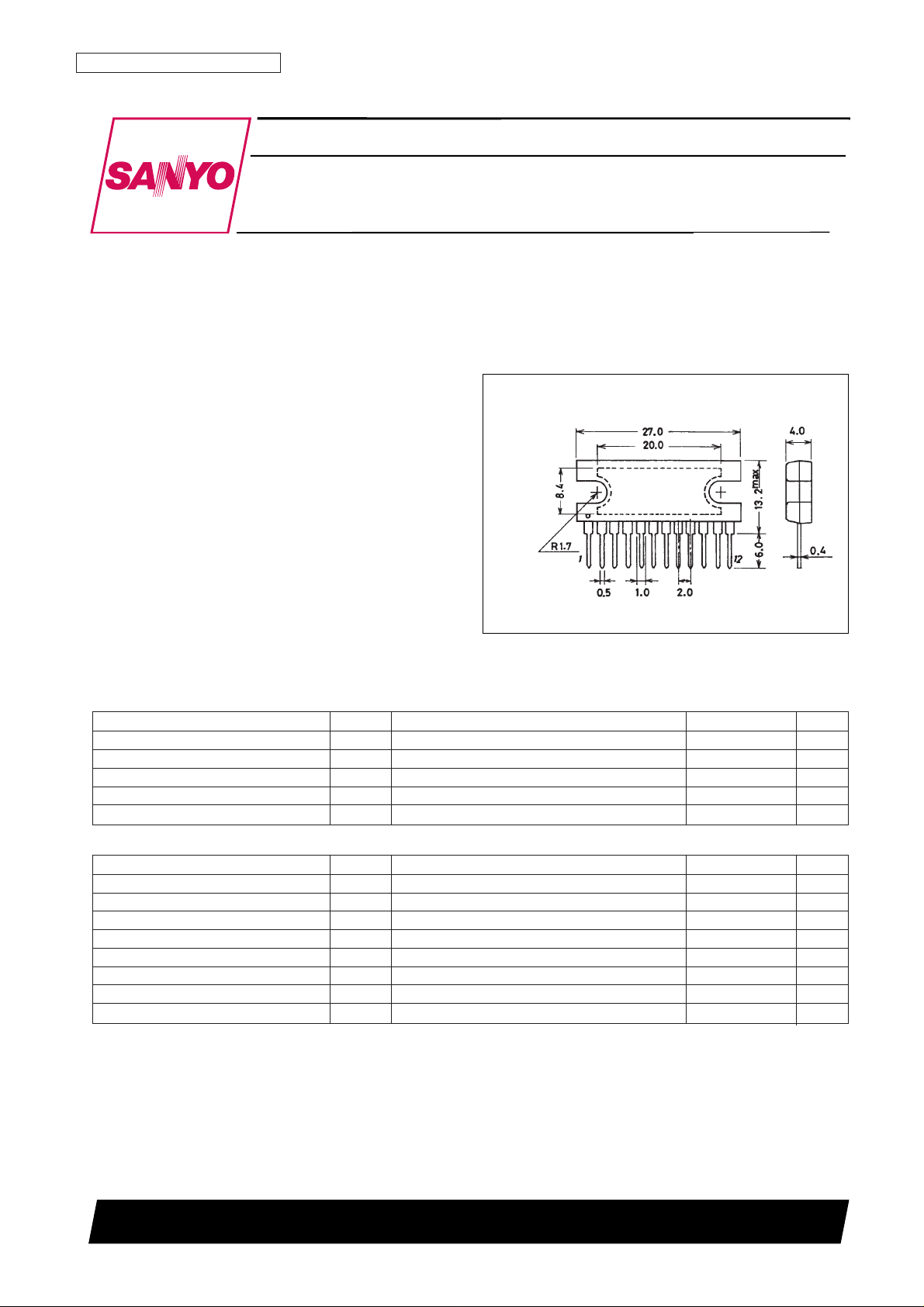
Package Dimensions
unit: mm
3049A-SIP12H
SANYO: SIP12H
[LA5620]
LA5620
SANYO Electric Co.,Ltd. Semiconductor Bussiness Headquarters
TOKYO OFFICE Tokyo Bldg., 1-10, 1 Chome, Ueno, Taito-ku, TOKYO, 110 JAPAN
Monolithic Linear IC
Specifications
Maximum Ratings at Ta = 25°C
Parameter Symbol Conditions Ratings Unit
Input voltage V
CC
6.25 to 12 V
PH5 output current I
PH5
0 to 1000 mA
B.BAK output current I
B.BAK
0 to 40 mA
ANA5 output current I
ANA5
0 to 100 mA
SYS3.3 output current I
SYS3.3
0 to 150 mA
S.RESET sink current I
SINK S
0 to 1 mA
P.DOWN sink current I
SINK P
0 to 1 mA
AC input current I
AC
0 to 1 mA
Operating Conditions at Ta = 25°C

Parameter Symbol Conditions
Ratings
Unit
min typ max
[PH5 Regulator Block] V
CC
= 10 V, I
PH5
= 1 A
Output voltage V
O PH5
4.75 5 5.25 V
Dropout voltage V
DROP PH5
– 0.5 1 V
Line regulation ∆V
OLN PH5
VCC= 6.25 to 12 V – – 200 mV
Load regulation ∆V
OLD PH5IPH5
= 0.5 to 1 A – – 200 mV
Peak output current I
OP
1.0 1.4 – A
Output shorted current I
OSC PH5
– 400 1000 mA
Current drain I
Q PH5
– 70 112 mA
[SYS3.3 Regulator Block] V
CC
= 10 V, I
SYS3.3
= 150 mA
Output voltage V
O SYS3.3
3.13 3.3 3.47 V
Dropout voltage V
DROP SYS3.3
– 2 2.5 V
Line regulation ∆V
OLN SYS3.3VCC
= 6.25 to 12 V – – 200 mV
Load regulation ∆V
OLD SYS3.3ISYS3.3
= 5 to 150 mA – – 200 mV
Peak output current I
OP SYS3.3
150 210 – mA
Output shorted current I
OSC SYS3.3
– 200 450 mA
Current drain I
Q SYS3.3
– 17.5 28 mA
[ANA5 Regulator Block] V
CC
= 10 V, I
ANA5
= 100 mA
Output voltage V
O ANA5
4.75 5 5.25 V
Dropout voltage V
DROP ANA5
– 0.5 1 V
Line regulation ∆V
OLN ANA5
VCC= 6.25 to 12 V – – 200 mV
Load regulation ∆V
OLD ANA5IANA5
= 5 to 100 mA – – 200 mV
Peak output current I
OP ANA5
100 140 – mA
Output shorted current I
OSC ANA5
– 40 100 mA
Current drain I
Q ANA5
– 17.5 28 mA
[B.BAK Regulator Block] V
CC
= 10 V, I
BAK
= 40 mA
Output voltage V
O BAK
3.13 3.3 3.47 V
Dropout voltage V
DROP BAK
– 2 2.5 V
Line regulation ∆V
OLN BAK
VCC= 6.25 to 12 V – – 200 mV
Load regulation ∆V
OLD BAKIBAK
= 5 to 40 mA – – 200 mV
Peak output current I
OP BAK
40 56 – mA
Output shorted current I
OSC BAK
– 40 120 mA
Current drain I
Q BAK
– 15 24 mA
BAK pin input current I
IN BAK
VCC= 0 V, V
BAK
= 3.3 V – – 100 nA
[P.DOWN Detection Circuit] V
CC
= 10 V
P.DOWN threshold voltage V
TH P.DOWN
3.0 3.16 3.32 V
P.DOWN residual voltage Vsat
P.DOWN
cd1 pin = shorted, P.DOWN pin = 1 mA – – 200 mV
P.DOWN delay time Td1 cd1 = 1 µF 75 100 125 ms
[S.RESET Detection Circuit] V
CC
= 10 V
S.RESET residual voltage V
TH S.RESET
cd1 pin = shorted, S.RESET pin = 1 mA – – 200 mV
S.RESET delay time Td2 cd2 = 1 µF 75 100 125 ms
[AC Detection Circuit] V
CC
= 10 V
AC threshold voltage V
TH AC
0.5 0.7 0.9 V
[STBY Detection Circuit] V
CC
= 10 V
STBY threshold voltage V
TH STBY
1.3 1.8 2.3 V
No. 5639-2/4
LA5620
Electrical Characteristics at Ta = 25°C
 Loading...