

Page 1
Ordering number :ENN5673
22500RM (OT) No. 5673-1/8
Overview
The LA5619M is a single-chip IC that integrates a battery
voltage detection function and a lead battery charger to
support compact sets.
Functions
• Charge voltage can be switched between cycle voltage
and trickle voltage (4.9 V typ. → 4.6 V typ.).
• Charge current limit can be set with an external resistor
(125 mA typ.).
• Built-in charge current detection circuit
• Built-in battery voltage detection circuit
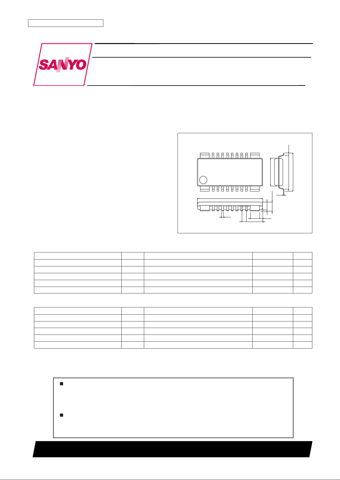
Package Dimensions
unit: mm
3097-MFP16FS
1
16
8
9
0.15
0.6251.35
0.35
1.0
2.8
12.6
5.4
1.8max
1.5
0.1
6.35
7.6
0.625
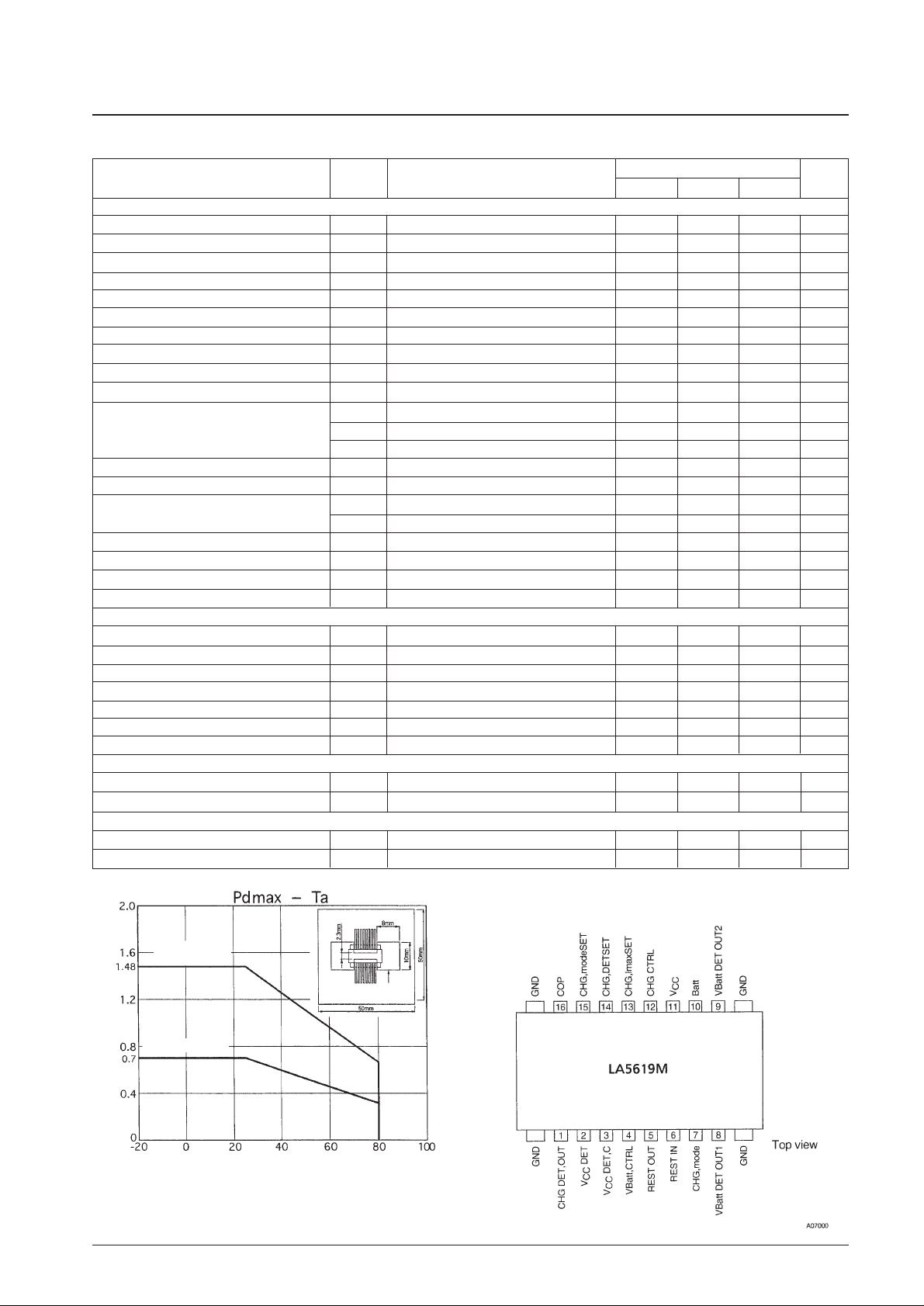
[LA5619M]
LA5619M
SANYO Electric Co.,Ltd. Semiconductor Company
TOKYO OFFICE Tokyo Bldg., 1-10, 1 Chome, Ueno, Taito-ku, TOKYO, 110-8534 JAPAN
Lead Battery Charger IC with Battery
Voltage Detection Function
Monolithic linear IC
SANYO: MFP16FS
Any and all SANYO products described or contained herein do not have specifications that can handle
applications that require extremely high levels of reliability, such as life-support systems, aircraft’s
control systems, or other applications whose failure can be reasonably expected to result in serious
physical and/or material damage. Consult with your SANYO representative nearest you before using
any SANYO products described or contained herein in such applications.
SANYO assumes no responsibility for equipment failures that result from using products at values that
exceed, even momentarily, rated values (such as maximum ratings, operating condition ranges, or other
parameters) listed in products specifications of any and all SANYO products described or contained
herein.
Parameter Symbol Conditions Ratings Unit
Supply voltage V
CC
max 15 V
Battery pin voltage
V
Battery
max
6V
Allowable power dissipation Pd max 0.7 W
Operating temperature Topr –20 to +80 °C
Storage temperature Tstg –30 to +125 °C
Specifications
Maximum Rating at Ta = 25°C
Parameter Symbol Conditions Ratings Unit
Supply voltage V
CC
5.5 to 14.5 V
Battery pin voltage V
Battery
IN 0 to 5.5 V
CHARGE LED sink current I
CHG-LED
0 to 40 mA
DET.LED sink current I
DET-LED
0 to 40 mA
V
BAT
sink current I
BAT-LED
0 to 40 mA
Operating Conditions at Ta = 25°C
Page 2
No. 5673-2/8
LA5619M
Parameter Symbol Conditions
Ratings
Unit
min typ max
[Charge System]
Charge voltage (when trickle is selected) V
O
1IO= 10 mA 4.4 4.6 4.7 V
Charge voltage (when cycle is selected) V
O
2IO= 50 mA 4.7 4.9 5.0 V
Differential charge voltage Vdif ∆V
O
= VO2– V
O1
0.2 0.3 0.4 V
Cycle → trickle switching current I
CT1
20 23 26 mA
Trickle → cycle switching current I
CT2
35 41 47 mA
Output peak current I
OP
RL= 33 Ω 112.5 125 137.5 mA
Line regulation (when trickle is selected) V
OLN1VCC
= 8 to 14.5 V, IO= 10 mA 50 100 mV
Line regulation (when cycle is selected) V
OLN2VCC
= 8 to 14.5 V, IO= 50 mA 100 150 mV
Load regulation (when trickle is selected) V
OLD1IO
= 0.5 to 30 mA 50 100 mV
Load regulation (when cycle is selected) V
OLD2IO
= 50 to 60 mA 100 150 mV
I
CC1IO
= 0 mA 6 10 mV
Current drain I
CC2IO
= 50 mA (I
CC2
includes IO) 65 73 mA
I
CC3RL
= 33 Ω (I
CC3
includes IO) 155 175 mA
CHG DET, OUT remaining voltage V
CHG-LEDIIN
= 40 mA 1.1 1.3 V
CHG DET, OUT leak voltage I
CHG-LEDVIN
= 9 V 200 nA
CHARGE detection current
I
CHG-DET1
on → off 0.15 0.25 0.35 mA
I
CHG-DET2
off → on 0.8 1.0 1.2 mA
VCC DET remaining voltage V
DETIIN
= 40 mA 1.1 1.3 V
VCC DET leak voltage I
DETVIN
= 9 V 200 nA
VCC DET detection voltage V
CC-DET
4.95 5.2 5.3 V
VCC DET hysteresis width
V
CC-DET, HYS
0.05 0.1 0.2 V
[Battery System]
Battery detection voltage V
Batt
3.17 3.3 3.43 V
V
Batt DET OUT1
pin’s remaining voltage
V
BAT-OUT1IIN
= 40 mA 0.3 0.5 V
V
Batt DET OUT1
pin’s leak current I
BAT-OUT1VIN
= 5 V 200 nA
Current drain when detection circuit is off
I
OFF
batt = 2.5 V 5 6 µA
Current drain when detection circuit is on
I
ON
No load 350 500 µA
Current drain during Battery SAVE I
SAVEVBatt CTRL
= 4 V 20 30 µA
V
Batt DET OUT2
pin’s remaining voltage
V
BAT-OUT2IIN
= 40 mA 1.1 1.3 V
[Internal Transistors for Reset]
REST OUT remaining voltage V
REST
REST.IN = 2 µA, IIN= 50 µA 0.3 0.5 V
REST OUT leak current I
RESTVIN
= 5 V 200 nA
[V
Batt CTRL
Pin]
Threshold voltage V
Batt-CTRL
1.10 1.27 1.50 V
V
Batt CTRL
pin input current I
Batt-CTRLVIN
= 4 V 17 24 µA
Operating Characteristics at Ta = 25°C, VCC= 9 V, Batt. IN = 4 V
Allowable power dissipation, Pd max — mW
Operating temperature, Ta — °C
Recommended
board mounting
Independent IC
Pin Assignment
Copper plating 180 mm
2
Board material: Paper phenol t = 1.5 mm
Page 3
No. 5673-3/8
LA5619M
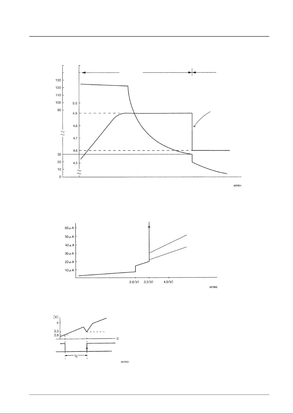
Battery Charger Charging Characteristics
Cycle charge
Current Drain Characteristics
Relationship between Reset and Battery Circuit
The V
Batt
circuit operates at the edge
where the reset voltage becomes Hi.
(At this time, the output transistors are
set on and the load is put on; If this
voltage is 3.3 [V] or higher, the V
Batt
circuit operates, and if it is lower than
3.3 [V], it does not start up.
Current limiting with current limiter
Charge current characteristics
Charge voltage characteristics
Detects charge current of 23 mA
and switches charge voltage
from 4.9 V to 4.6 V
* Charge current is variable
Trickle charge
Charging time
Charge current
Battery pin voltage
(+Vbat circuit current)
Reset on
Batt SAVE on current
Reset off current
(+reset circuit current)
Battery
voltage
Rest voltage 2.8 [V]
3.3 [V] or higher
Page 4

No. 5673-4/8
LA5619M
Cycle ↔ Trickle Switching Hysteresis
Charge current I
Batt
[mA]
Charge current V
Batt
[V]
Charge Detection Hysteresis
Charge current I
Batt
[mA]
LED on
LED off
Page 5

No. 5673-5/8
LA5619M
Timing Charts
(Battery provided)
(Battery only)
Page 6

No. 5673-6/8
LA5619M
Block Diagram
Notes: 1. Use capacitors with little temperature-related capacitance fluctuation.
2. Do not provide capacitors to the Batt pin (Pin 10)
3. The reset IC must be provided externally.
Overdrive
control
GND (frame)
Reset IC
OUT
To current limiter
Page 7

No. 5673-7/8
LA5619M
Battery detection voltage, V
Batt
— V
Battery detection voltage, V
Batt
— V
V
CCDET
voltage, V
CCDET
— V
V
CHGDETOUT
voltage, V
CHGDETOUT
— V
V
CHGmode
voltage, V
CHGmode
— V
V
BattDETOUT2
voltage, V
BattDETOUT2
— V
Battery detection voltage, V
Batt
— V
Output peak current, Iop — mA
Operating temperature, Ta — °C Operating temperature, Ta — °C
Charge current, I
Batt
— mA Battery pin voltage, V
Batt
— V
Charge current, I
Batt
— mA
Supply voltage, V
CC
— V
Charge current, I
Batt
— mA
Supply voltage, VCC— V
Cycle selected (75 Ω load)
Trickle selected (no load)
LED off
LED off
LED off
LED off
LED on
LED on
LED on
LED on
Page 8

This catalog provides information as of February, 2000. Specifications and information herein are subject
to change without notice.
Specifications of any and all SANYO products described or contained herein stipulate the performance,
characteristics, and functions of the described products in the independent state, and are not guarantees
of the performance, characteristics, and functions of the described products as mounted in the customer’s
products or equipment. To verify symptoms and states that cannot be evaluated in an independent device,
the customer should always evaluate and test devices mounted in the customer’s products or equipment.
SANYO Electric Co., Ltd. strives to supply high-quality high-reliability products. However, any and all
semiconductor products fail with some probability. It is possible that these probabilistic failures could
give rise to accidents or events that could endanger human lives, that could give rise to smoke or fire,
or that could cause damage to other property. When designing equipment, adopt safety measures so
that these kinds of accidents or events cannot occur. Such measures include but are not limited to protective
circuits and error prevention circuits for safe design, redundant design, and structural design.
In the event that any or all SANYO products (including technical data, services) described or contained
herein are controlled under any of applicable local export control laws and regulations, such products must
not be exported without obtaining the export license from the authorities concerned in accordance with the
above law.
No part of this publication may be reproduced or transmitted in any form or by any means, electronic or
mechanical, including photocopying and recording, or any information storage or retrieval system,
or otherwise, without the prior written permission of SANYO Electric Co., Ltd.
Any and all information described or contained herein are subject to change without notice due to
product/technology improvement, etc. When designing equipment, refer to the “Delivery Specification”
for the SANYO product that you intend to use.
Information (including circuit diagrams and circuit parameters) herein is for example only; it is not
guaranteed for volume production. SANYO believes information herein is accurate and reliable, but
no guarantees are made or implied regarding its use or any infringements of intellectual property rights
or other rights of third parties.
PS No. 5673-8/8
LA5619M
 Loading...