

Page 1
Ordering number : EN4786
20695TH (OT) No. 4786-1/8
Overview
The LA5609 is a multi-function multi-voltage power
supply that includes a built-in on/off function. The
LA5609 provides dedicated outputs for motors, audio
systems, CD drive, radio, microprocessor, and loading
drives, thus making it optimal for use as the system power
supply in radio cassette recorders with CD player.
Functions
• Power supply systems for radio cassette recorders with
CD player
• Miniature electronic equipment
• Low-saturation regulator (14.5 V/1.2 A, 9 V/300 mA,
7.5 V/800 mA)
• High-precision power supply (two 5 V/220 mA systems,
5 V/100 mA, 8 V/800 mA)
• Limiter power supply (9 V/60 mA)
Features
• Supports end-product miniaturization by the provision
of built-in control circuits.
• Provides reduced internal power dissipation by the
adoption of a low-saturation regulator.
• Built-in output current limiter prevents IC destruction
due to output shorts.
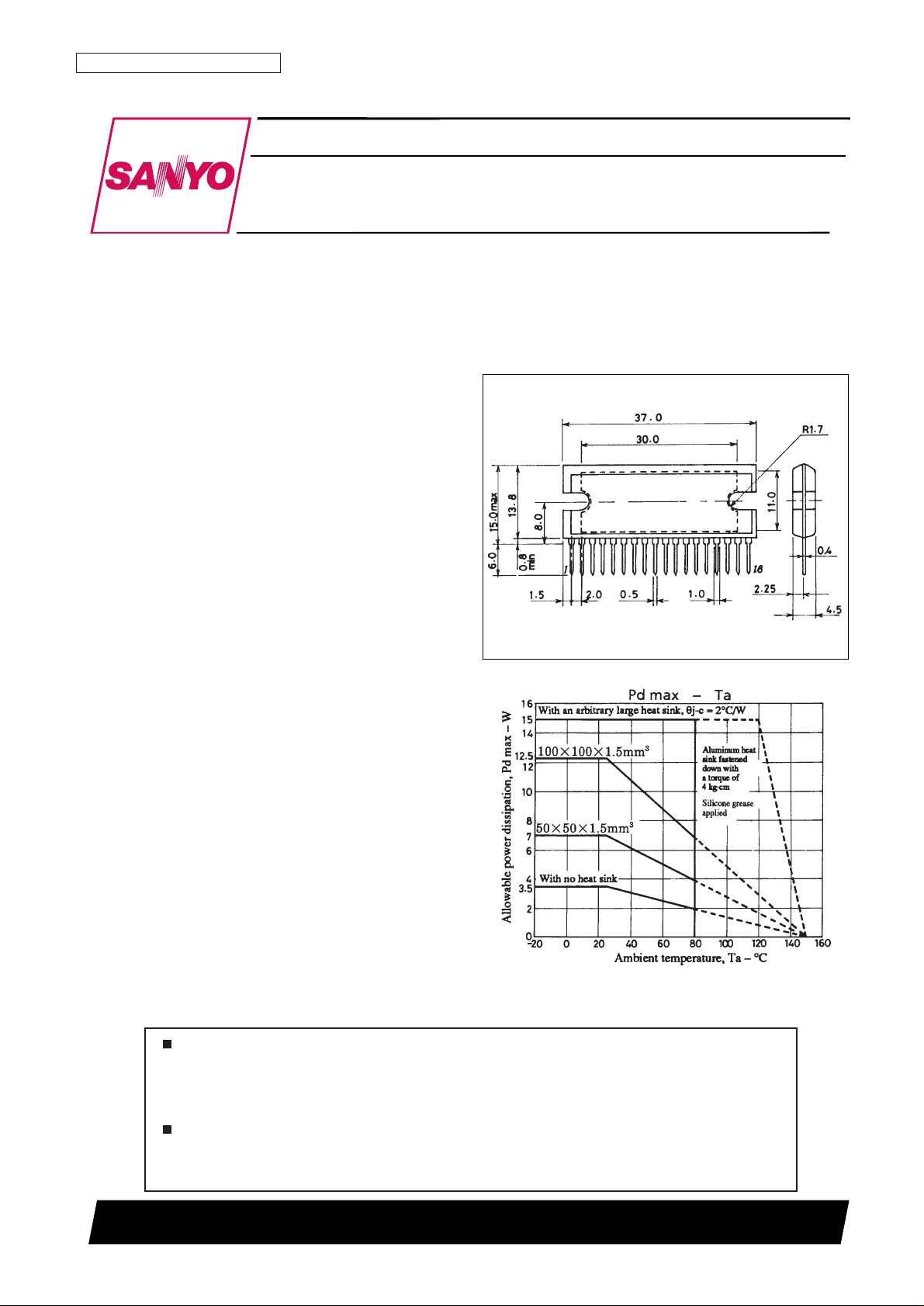
Package Dimensions
unit: mm
3109-SIP18H
SANYO: SIP18H
[LA5609]
LA5609
SANYO Electric Co.,Ltd. Semiconductor Bussiness Headquarters
TOKYO OFFICE Tokyo Bldg., 1-10, 1 Chome, Ueno, Taito-ku, TOKYO, 110-8534 JAPAN
Multi-Function Voltage Regulator
for Radio Cassette Recorders with CD Player
Monolithic Linear IC
Any and all SANYO products described or contained herein do not have specifications that can handle
applications that require extremely high levels of reliability, such as life-support systems, aircraft’s
control systems, or other applications whose failure can be reasonably expected to result in serious
physical and/or material damage. Consult with your SANYO representative nearest you before using
any SANYO products described or contained herein in such applications.
SANYO assumes no responsibility for equipment failures that result from using products at values that
exceed, even momentarily, rated values (such as maximum ratings, operating condition ranges, or other
parameters) listed in products specifications of any and all SANYO products described or contained
herein.
Page 2
Specifications
Maximum Ratings at Ta = 25°C
Operating Conditions at Ta = 25°C
Operating Characteristics at Ta = 25°C in the specified test circuit
No. 4786-2/8
LA5609
Parameter Symbol Conditions Ratings Unit
Input voltage V
CC
max 24 V
V
REF
pin voltage V
REF
6 V
POWER CONT pin voltage V
CONT
max 6 V
AC STBY pin voltage V
AC
max 6 V
MODE SW pin voltage V
MODE
max 6 V
Allowable power dissipation Pd max With no heat sink 3.5 W
Operating temperature Topr –20 to +80 °C
Storage temperature Tstg –55 to +150 °C
Parameter Symbol Conditions Ratings Unit
Input voltage V
CC
6.5 to 22 V
Input voltage V
REF
4.5 to 5.5 V
Motor 14.5 V output current I
O MOT
0 to 1.2 A
Audio 9 V output current I
O AUD
0 to 300 mA
Digital 5 V output current I
O DIGI
0 to 220 mA
CD 5 V output current I
O CD5
0 to 220 mA
CD 8 V output current I
O CD8
0 to 0.8 A
Radio 5 V output current I
O RAD
0 to 100 mA
Loading 7.5 V output current I
O LOAD
0 to 0.8 A
9 V limiter output current I
O LIM
0 to 60 mA
Parameter Symbol Conditions min typ max Unit
[No Load Currents]
V
CC
quiescent current I
CC
VCC= 12 V, Power cont.: L, 5 V
REF
: L 500 µA
Influx 1 V
REF
5 V input current I
REF1
VCC= 0 V, Power cont.: L 10 µA
Influx 2 V
REF
5 V input current I
REF2
VCC= 12 V, Power cont. = 5 V 700 µA
[Motor 14.5 V Regulator Block] V
CC
= 16 V, I
O MOT
= 1.2 A, Power cont. = 5 V
Output voltage V
O MOT
14.0 14.5 15.0 V
Dropout voltage V
DROP-MOTVCC
= 14 V, I
O MOT
= 600 mA 0.4 0.8 V
Line regulation ∆V
OLN-MOTVCC
= 16 to 22 V 30 300 mV
Load regulation ∆V
OLD-MOTIO MOT
= 0 to 1.2 A 200 800 mV
Peak output current I
OP-MOT
1.2 A
Short circuit output current I
OSC-MOT
300 mA
[Audio 9 V Regulator Block] V
CC
= 11 V, I
O AUD
= 300 mA, Power cont. = 5 V
Output voltage V
O AUD
8.5 9.0 9.5 V
Dropout voltage V
DROP-AUDVCC
= 8.5 V, I
O AUD
= 150 mA 0.2 0.8 V
Line regulation ∆V
OLN-AUDVCC
= 11 to 22 V 100 400 mV
Load regulation ∆V
OLD-AUDIO AUD
= 0 to 300 mA 100 400 mV
Peak output current I
OP-AUD
300 mA
Short circuit output current I
OSC-AUD
50 mA
Ripple rejection R
REJ-AUD
f = 120 Hz, 10 V ≤ VCC≤ 15 V, C = 1 µF 60 dB
Continued on next page.
Page 3
Continued from preceding page.
No. 4786-3/8
LA5609
Parameter Symbol Conditions min typ max Unit
[Digital 5.0 V Regulator Block] Power cont. = 5 V
Output voltage V
O DIGIVCC
= 16 V, I
O DIGI
= 100 mA 4.95 5.05 5.15 V
Dropout voltage V
DROP-DIGIVCC
= 4.9 V, I
O DIGI
= 110 mA 0.6 1.4 V
∆V
OLN1-DIGIVCC
= 16 to 20 V, I
O DIGI
= 220 mA 0 40 60 mV
Line regulation
∆V
OLN2-DIGIVCC
= 16 to 8 V, I
O DIGI
= 220 mA –100 –70 0 mV
∆V
OLN3-DIGIVCC
= 16 to 20 V, I
O DIGI
= 0 mA –20 0 +20 mV
∆V
OLN4-DIGIVCC
= 16 to 8 V, I
O DIGI
= 0 mA –20 0 +20 mV
Load regulation
∆V
OLD1-DIGIVCC
= 16 V, I
O DIGI
= 100 to 220 mA 0 40 60 mV
∆V
OLD2-DIGIVCC
= 16 V, I
O DIGI
= 100 to 0 mA –60 –40 0 mV
Peak output current I
OP-DIGIVCC
= 6.5 V 220 260 mA
Short circuit output current I
OSC-DIGIVCC
= 6.5 V 260 mA
[CD 5.0 V Regulator Block] Power cont. = 5 V, Mode SW = 5 V
Output voltage V
O CD5VCC
= 16 V, I
O CD5
= 100 mA 4.9 5.0 5.1 V
Dropout voltage V
DROP-CD5VCC
= 4.9 V, I
O CD5
= 110 mA 0.6 1.4 V
∆V
OLN1-CD5VCC
= 16 to 20 V, I
O CD5
= 220 mA 0 40 60 mV
Line regulation
∆V
OLN2-CD5VCC
= 16 to 8 V, I
O CD5
= 220 mA –100 –70 0 mV
∆V
OLN3-CD5VCC
= 16 to 20 V, I
O CD5
= 0 mA –20 0 +20 mV
∆V
OLN4-CD5VCC
= 16 to 8 V, I
O CD5
= 0 mA –20 0 +20 mV
Load regulation
∆V
OLD1-CD5VCC
= 16 V, I
O CD5
= 100 to 220 mA 0 40 60 mV
∆V
OLD2-CD5VCC
= 16 V, I
O CD5
= 100 to 0 mA –60 –40 0 mV
Peak output current I
OP-CD5VCC
= 6.5 V 220 260 mA
Short circuit output current I
OSC-CD5VCC
= 6.5 V 260 mA
[CD 8.0 V Regulator Block] V
CC
= 9.5 V, I
O CD8
= 800 mA, Power cont. = 5 V, Mode SW = 5 V
Output voltage V
O CD8
7.5 8.0 8.5 V
Dropout voltage V
DROP-CD8VCC
= 7.5 V, I
O CD8
= 400 mA 0.6 1.4 V
Line regulation ∆V
OLN-CD8VCC
= 9.5 to 22 V 20 200 mV
Load regulation ∆V
OLD-CD8IO CD8
= 0 to 800 mA 100 250 mV
Peak output current I
OP-CD8
0.8 1.1 A
[Radio 5.0 V Regulator Block] Power cont. = 5 V
Output voltage V
O RADVCC
= 16 V, I
O RAD
= 50 mA 4.9 5.0 5.1 V
Dropout voltage V
DROP-RADVCC
= 4.9 V, I
O RAD
= 50 mA 0.6 1.4 V
∆V
OLN1-RADVCC
= 16 to 20 V, I
O RAD
= 100 mA 0 20 40 mV
Line regulation
∆V
OLN2-RADVCC
= 16 to 8 V, I
O RAD
= 100 mA –70 –40 0 mV
∆V
OLN3-RADVCC
= 16 to 20 V, I
O RAD
= 0 mA –10 0 +10 mV
∆V
OLN4-RADVCC
= 16 to 8 V, I
O RAD
= 0 mA –10 0 +10 mV
Load regulation
∆V
OLD1-RADVCC
= 16 V, I
O RAD
= 50 to 100 mA 0 20 40 mV
∆V
OLD2-RADVCC
= 16 V, I
O RAD
= 50 to 0 mA –40 –20 0 mV
Peak output current I
OP-RADVCC
= 6.5 V 100 160 mA
Short circuit output current I
OSC-RADVCC
= 6.5 V 160 mA
[Loading 7.5 V Regulator Block] Power cont. = 5 V
REG SET voltage V
REGSVCC
= 16 V, I
O LOAD
= 400 mA 1.27 1.31 1.35 V
Dropout voltage V
DROP-LOADVCC
= 7.3 V, I
O LOAD
= 400 mA 0.4 0.8 V
∆V
OLN1-LOADVCC
= 16 to 20 V, I
O LOAD
= 800 mA 0 10 20 mV
Line regulation
∆V
OLN2-LOADVCC
= 16 to 9 V, I
O LOAD
= 800 mA –20 –10 0 mV
∆V
OLN3-LOADVCC
= 16 to 20 V, I
O LOAD
= 0 mA –10 0 +10 mV
∆V
OLN4-LOADVCC
= 16 to 9 V, I
O LOAD
= 0 mA –10 0 +10 mV
Load regulation
∆V
OLD1-LOADVCC
= 16 V, I
O LOAD
= 400 to 800 mA 0 10 20 mV
∆V
OLD2-LOADVCC
= 16 V, I
O LOAD
= 400 to 0 mA –20 –10 0 mV
Peak output current I
OP-LOADVCC
= 9 V 0.8 A
Short circuit output current I
OSC-LOADVCC
= 9 V 200 mA
Continued on next page.
Page 4
Continued from preceding page.
Timing Chart
No. 4786-4/8
LA5609
Parameter Symbol Conditions min typ max Unit
[9.0 V Limiter Block] V
CC
= 11 V, I
O LIM
= 60 mA
Output voltage V
O LIM
8.0 9.0 9.5 V
Dropout voltage V
DROP-LIMVCC
= 8 V 1.0 V
Peak output current I
OP-LIM
60 150 mA
Short circuit output current I
OSC-LIM
200 mA
[Mode Switch] V
CC
= 12 V
Voltage with radio mode on V
MTH H
Voltage when the radio output is switched high 1.1 1.4 1.7 V
Voltage with radio mode off V
MTH L
Voltage when the radio output is switched low 2.9 3.1 3.3 V
Voltage with CD mode on V
RTH H
Voltage when the CD 5 V and CD 8 V are switched high 2.9 3.1 3.3 V
Input impedance Z
I
16.8 24 31.2 kΩ
[Power Control] V
CC
= 12 V
Output on control voltage V
I CONT-ON
3.0 V
Output off control voltage V
I CONT-OFF
2.0 V
[AC standby]
Output on control voltage V
I AC-ON
2.0 V
Output off control voltage V
I AC-OFF
1.0 V
[5 V System Regulator Block] V
CC
= 16 V, I
O DIGI
= I
O CD5
= 100 mA, I
O RAD
= 50 mA
Difference between
∆V
DEF
0 0.15 V
output voltages
Page 5
Function Table
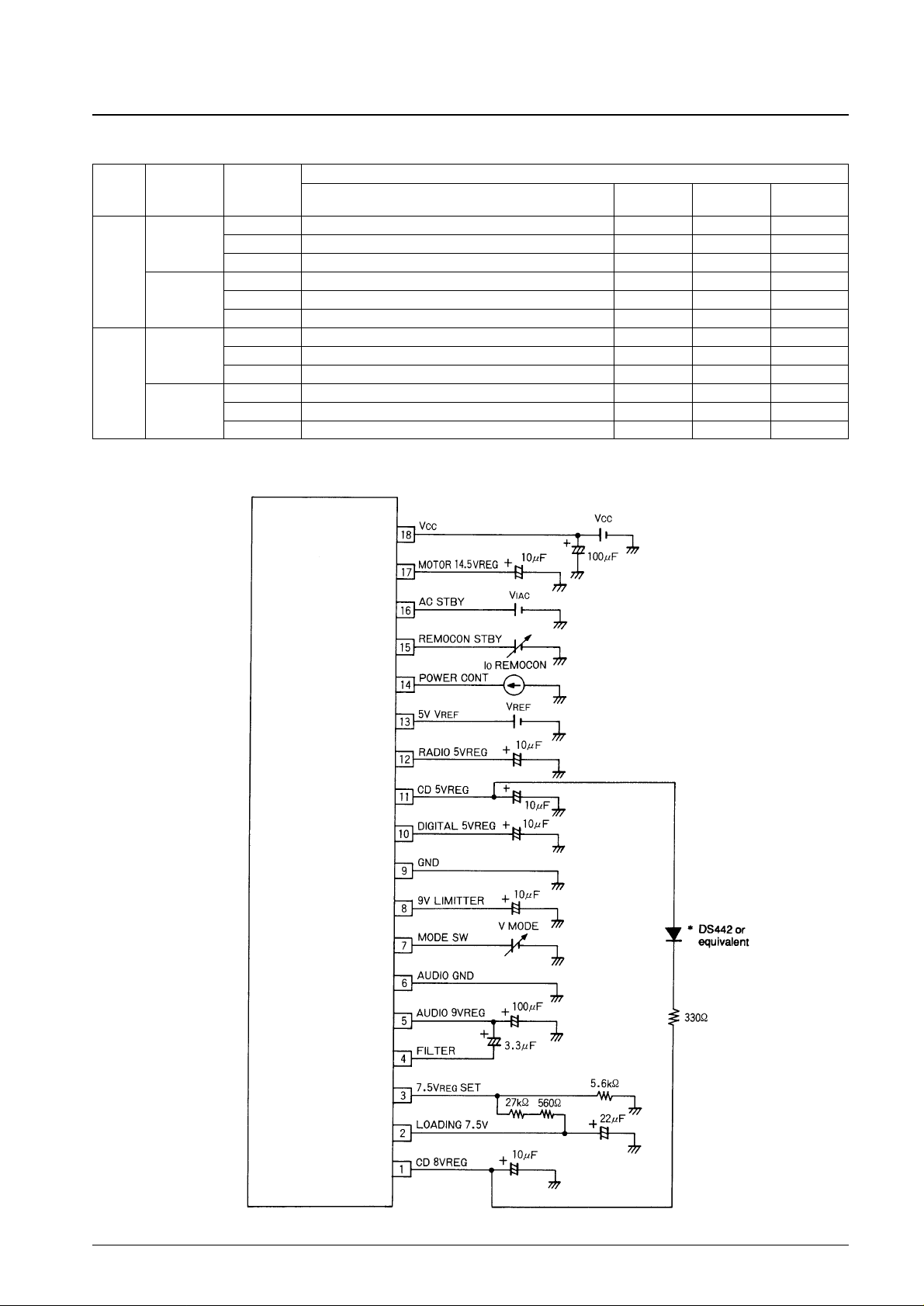
Test Circuit
Note: * This diode is required for bringing up the CD 8 V regulator.
No. 4786-5/8
LA5609
V
OUT
V
REF
Power cont. Mode SW Audio Motor Digital Loading CD 8 V/ Radio Limitter
9 V 14.5 V 5 V 7.5 V CD 5 V 5 V 9 V
L (0 V) L L L H
L M (2.5 V) L L L H
L
H (5 V) L L L H
L (0 V) L L L H
H M (2.5 V) L L L H
H (5 V) L L L H
L (0 V) L L L H
L M (2.5 V) L L L H
H
H (5 V) L L L H
L (0 V) H L L H
H M (2.5 V) H L H H
H (5 V) H H L H
Page 6
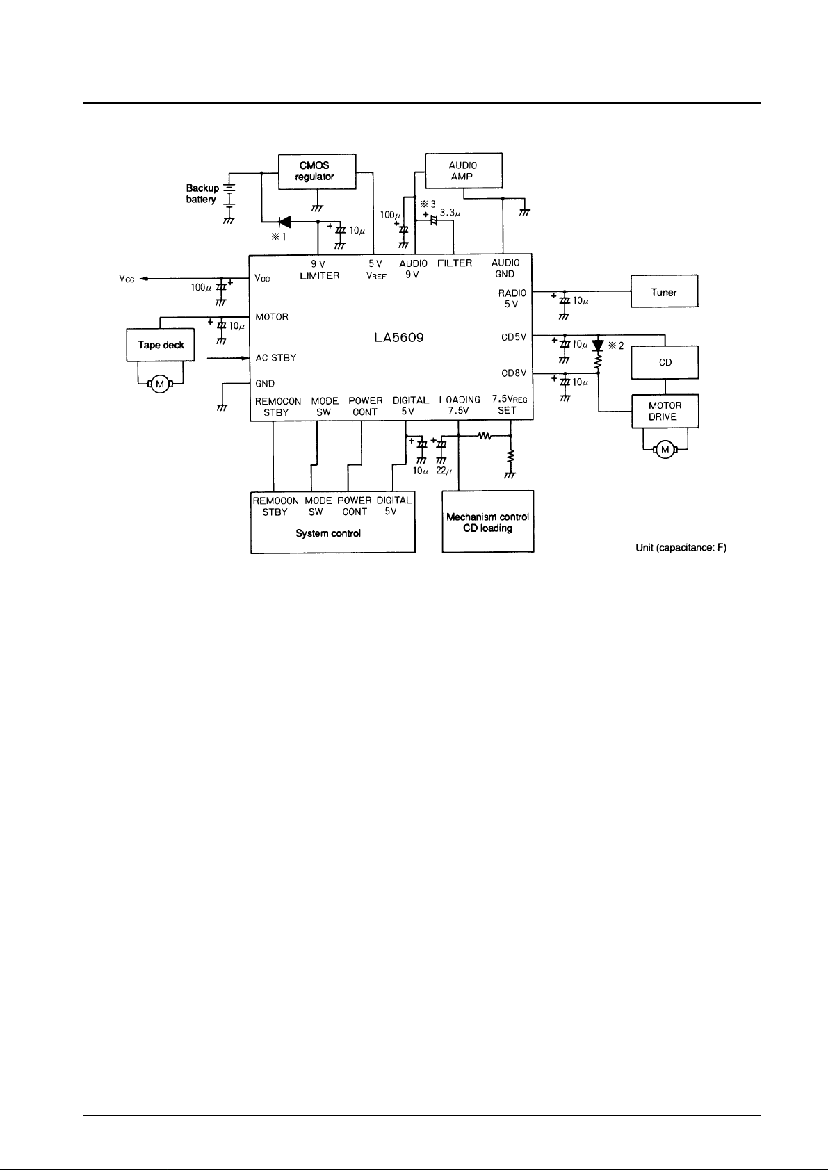
Sample Application Circuit
Note: 1. The diode in the 9 V limiter block must be added. It is required for preventing current from flowing into the 9 V limiter from the backup battery when
V
CC
is off.
2. The diode and resistor between the CD 5 V and CD 8 V blocks must be added. It is required to bring up the CD 8 V regulator.
3. External noise can be limited and ripple rejection can be improved by adding an electrolytic capacitor between the audio 9 V and the filter circuits.
4. The electrolytic capacitors between V
CC
and GND and between each V0 and GND should have capacitances at least those shown in the diagram.
Use Sanyo HW Series aluminum electrolytic capacitors or equivalent products.
No. 4786-6/8
LA5609
Page 7
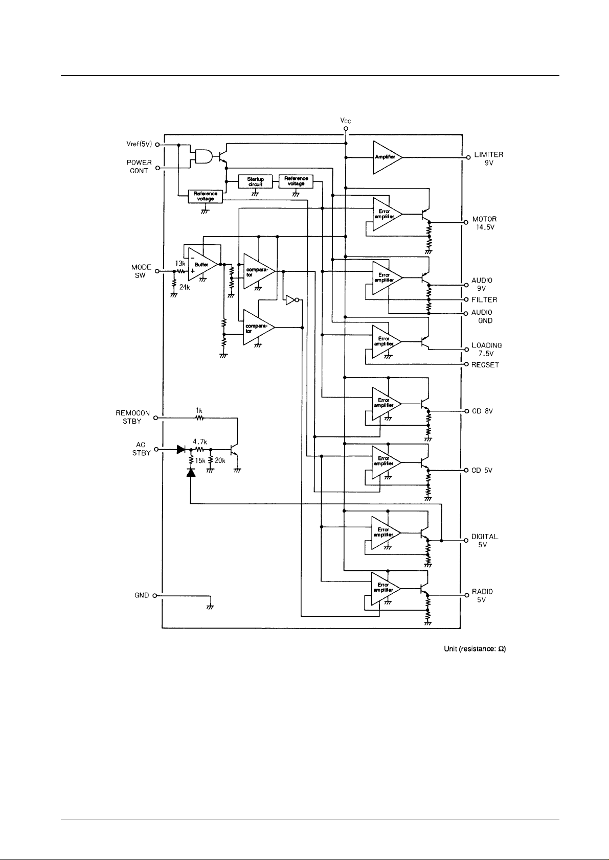
Equivalent Circuit Block Diagram
No. 4786-7/8
LA5609
Page 8
PS No. 4786-8/8
LA5609
This catalog provides information as of August, 1998. Specifications and information herein are subject to
change without notice.
Specifications of any and all SANYO products described or contained herein stipulate the performance,
characteristics, and functions of the described products in the independent state, and are not guarantees
of the performance, characteristics, and functions of the described products as mounted in the customer’s
products or equipment. To verify symptoms and states that cannot be evaluated in an independent device,
the customer should always evaluate and test devices mounted in the customer’s products or equipment.
SANYO Electric Co., Ltd. strives to supply high-quality high-reliability products. However, any and all
semiconductor products fail with some probability. It is possible that these probabilistic failures could
give rise to accidents or events that could endanger human lives, that could give rise to smoke or fire,
or that could cause damage to other property. When designing equipment, adopt safety measures so
that these kinds of accidents or events cannot occur. Such measures include but are not limited to protective
circuits and error prevention circuits for safe design, redundant design, and structural design.
In the event that any and all SANYO products described or contained herein fall under strategic
products (including services) controlled under the Foreign Exchange and Foreign Trade Control Law of
Japan, such products must not be exported without obtaining export license from the Ministry of
International Trade and Industry in accordance with the above law.
No part of this publication may be reproduced or transmitted in any form or by any means, electronic or
mechanical, including photocopying and recording, or any information storage or retrieval system,
or otherwise, without the prior written permission of SANYO Electric Co., Ltd.
Any and all information described or contained herein are subject to change without notice due to
product/technology improvement, etc. When designing equipment, refer to the “Delivery Specification”
for the SANYO product that you intend to use.
Information (including circuit diagrams and circuit parameters) herein is for example only; it is not
guaranteed for volume production. SANYO believes information herein is accurate and reliable, but
no guarantees are made or implied regarding its use or any infringements of intellectual property rights
or other rights of third parties.
 Loading...