

Page 1
Ordering number : EN4370A
93098TH (OT) / N1694TH (OT) AX-9952 No. 4370-1/6
LA5606N
SANYO Electric Co.,Ltd. Semiconductor Bussiness Headquarters
TOKYO OFFICE Tokyo Bldg., 1-10, 1 Chome, Ueno, Taito-ku, TOKYO, 110-8534 JAPAN
BS/CS Tuner Regulator with On/Off Function
Monolithic Linear IC
Any and all SANYO products described or contained herein do not have specifications that can handle
applications that require extremely high levels of reliability, such as life-support systems, aircraft’s
control systems, or other applications whose failure can be reasonably expected to result in serious
physical and/or material damage. Consult with your SANYO representative nearest you before using
any SANYO products described or contained herein in such applications.
SANYO assumes no responsibility for equipment failures that result from using products at values that
exceed, even momentarily, rated values (such as maximum ratings, operating condition ranges, or other
parameters) listed in products specifications of any and all SANYO products described or contained
herein.
Overview
The LA5606N is a low saturation regulator IC for BS/CS
tuner applications, equipped with four regulators capable
of ON/OFF control.
Applications
• BS/CS tuner power supply system.
• Audio Video (AV) equipment with BS/CS receivers.
• Compact electronic equipment.
Functions
• Four low saturation regulators (15.7 V/300 mA,
12 V/150 mA, 9 V/100 mA and 5 V/500 mA).
• Output on/off control (“L” active).
• On-chip protective circuitry (current limiter, thermal
shutdown).
Features
• Supports compact set design while incorporating four
regulators needed by BS/CS tuners.
• Flexible system design by independent on/off control of
VO1, VO4, as well as VO2 and VO3 pair.
• Reduces internal loss by employment of low saturation
regulators.
• Adapting three input pins contributes power dissipation
reduction and heat sink design.
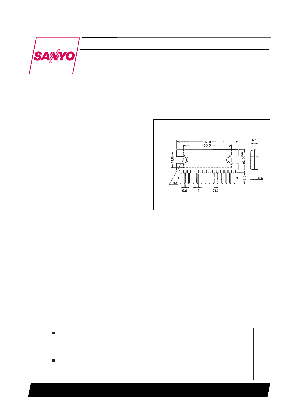
Package Dimensions
unit: mm
3023A-SIP14H
[LA5606N]
SANYO: SIP14H
Page 2
No. 4370-2/6
LA5606N
Parameter Symbol Conditions
Ratings
Unit
min typ max
Regulator 1 (V
EN
1 = low, VO1: ON, VIN1 = 18.7 V and IO1 = 300 mA)
Output voltage 1 V
O
1 14.9 15.7 16.5 V
Dropout voltage
V
DROP1-1
0.3 0.5 V
V
DROP1-2IO
1 = 150 mA 0.15 0.3 V
Line regulation ∆V
OLN
1 17.5 V ≤ VIN1 ≤ 23 V 20 100 mV
Load regulation ∆V
OLD
1 5 mA ≤ IO1 ≤ 300 mA 40 200 mV
Peak output current I
OP
1 350 540 mA
Output short current I
OSC
1 150 mA
Output on control voltage V
ENL
1 VO1: On 1.0 V
Output off control voltage V
ENH
1 VO1: Off 4.0 VIN1 V
Output low level voltage V
O
1 OFF 0.2 V
Output noise voltage V
NO
1 10 Hz ≤ f ≤ 100 kHz 110 µVrms
Ripple rejection Rrej1 f = 120 Hz, 18 V ≤ V
IN
1 ≤ 23 V 50 dB
Regulator 2 (V
EN
2 = low, VO2: ON, VIN2 = 15.0 V, IO2 = 150 mA)
Output voltage 2 V
O
2 11.4 12.0 12.6 V
Dropout voltage V
DROP
2 0.3 0.5 V
Line regulation ∆V
OLN
2 12.6 V ≤ VIN2 ≤ 23 V 20 100 mV
Load regulation ∆V
OLD
2 1 mA ≤ IO2 ≤ 150 mA 20 70 mV
Peak output current I
OP
2 200 270 mA
Output short current I
OSC
2 70 mA
Output on control voltage V
ENL
2 VO2: On 1.0 V
Output off control voltage V
ENH
2 VO2 :Off 4.0 VIN2 V
Output low level voltage V
O
2OFF 0.2 V
Output noise voltage V
NO
2 10 Hz ≤ f ≤ 100 kHz 110 µVrms
Ripple rejection Rrej2 f = 120 Hz, 13 V ≤ V
IN
2 ≤ 23 V 50 dB
Regulator 3 (V
EN
2 = low, VO3: ON, VIN2 = 12 V, IO3 = 100 mA)
Output voltage 3 V
O
3 8.55 9.0 9.45 V
Dropout voltage V
DROP
3 0.3 0.5 V
Line regulation ∆V
OLN
3 10.45 V ≤ VIN2 ≤ 23 V 20 100 mV
Load regulation ∆V
OLD
3 1 mA ≤ IO3 ≤ 100 mA 20 50 mV
Peak output current I
OP
3 150 180 mA
Output short current I
OSC
3 40 mA
Output on control voltage V
ENL
2 VO3: On 1.0 V
Output off control voltage V
ENH
2 VO3: Off 4.0 VIN2 V
Output low level voltage V
O
3 OFF 0.2 V
Output noise voltage V
NO
3 10 Hz ≤ f ≤ 100 kHz 70 µVrms
Ripple rejection Rrej3 f = 120 Hz, 11 V ≤ V
IN
2 ≤ 23 V 55 dB
Specifications
Maximum Ratings at Ta = 25°C
Operating Conditions at Ta = 25°C
Parameter Symbol Conditions Ratings Unit
Maximum input voltage V
IN
max VIN1 ≥ VIN2 ≥ VIN3 35 V
Enable pin voltage V
EN
max EN1, EN2, EN3 VINmax V
Allowable power dissipation Pd max
With infinite heat sink 15 W
With no heat sink 4.3 W
Operating temperature Topr –20 to +80 °C
Storage temperature Tstg –55 to +150 °C
Parameter Symbol Conditions Ratings Unit
Output current 1 I
O
1 Regulator 1 5 to 350 mA
Output current 2 I
O
2 Regulator 2 1 to 200 mA
Output current 3 I
O
3 Regulator 3 1 to 150 mA
Output current 4 I
O
4 Regulator 4 5 to 500 mA
Operating Characteristics at Ta = 25°C and the specified Test Circuit
Continued on next page.
Page 3

Pin Assignment
Note: The NC pins should not be used (No. 1 and No. 14 in the pin layout).
No. 4370-3/6
LA5606N
Parameter Symbol Conditions
Ratings
Unit
min typ max
Regulator 4 (V
EN
3 = low, VO4: ON, VIN3 = 8.0 V, IO4 = 500 mA)
Output voltage 4 V
O
4 4.75 5.0 5.25 V
Dropout voltage
V
DROP4-1
0.3 0.5 V
V
DROP4-2IO
4 = 250 mA 0.2 0.4 V
Line regulation ∆V
OLN
4 6.25 V ≤ VIN3 ≤ 23 V 20 100 mV
Load regulation ∆V
OLD
4 5 mA ≤ IO4 ≤ 500 mA 30 150 mV
Peak output current I
OP
4 500 900 mA
Output short current I
OSC
4 250 mA
Output on control voltage V
ENL
3 VO4: On 1.0 V
Output off control voltage V
ENH
3 VO4: Off 4.0 VIN3 V
Output low level voltage V
O
4 OFF 0.2 V
Output noise voltage V
NO
4 10 Hz ≤ f ≤ 100 kHz 70 µVrms
Ripple rejection Rrej4 f = 120 Hz, 7 V ≤ V
IN
3 ≤ 23 V 60 dB
Current dissipation 1 I
Q
1 IO1, IO2, IO3, IO4 = 0 11 mA
Current dissipation 2 I
Q
2
I
O
1 = 300mA, IO2 = 150 mA,
53 mA
I
O
3 = 100mA, IO4 = 500 mA
Continued from preceding page.
Page 4

Block Diagram
TSD: Thermal Shutdown Circuit
ON/OFF: Output on/off Control Circuit
CL: Current Limiter Circuit
No. 4370-4/6
LA5606N
Unit (resistance: Ω)
Page 5

Test Circuit
Function Table
The following table indicates conditions for operation with VIN1 ≥ VIN2 ≥ VIN3 (VIN1 ≥ 11 V, VIN2 ≥ 6 V and VIN3 ≥ 4 V).
1. Within the table of EN “H” indicates an H level and “L” indicates an L level.
2. In the table of VO“H” indicates an output on voltage while “L” indicates an output off voltage.
3. All output voltages corresponding to all EN locations are controlled independently.
(EN1 →VO1, EN2 → VO2 and VO3 , EN3 → VO4)
4. When EN is open, VO is at the H level.
EN (On/Off Control) Input Equivalent Block Diagram
VO1 (VO4) VO2 and VO3
No. 4370-5/6
LA5606N
Unit (capacitance: F)
EN1, EN2, EN3 VO1, VO2/VO3, VO4
H L
L H
Unit (resistance: Ω)
Page 6

PS No. 4370-6/6
LA5606N
This catalog provides information as of September, 1998. Specifications and information herein are
subject to change without notice.
Specifications of any and all SANYO products described or contained herein stipulate the performance,
characteristics, and functions of the described products in the independent state, and are not guarantees
of the performance, characteristics, and functions of the described products as mounted in the customer’s
products or equipment. To verify symptoms and states that cannot be evaluated in an independent device,
the customer should always evaluate and test devices mounted in the customer’s products or equipment.
SANYO Electric Co., Ltd. strives to supply high-quality high-reliability products. However, any and all
semiconductor products fail with some probability. It is possible that these probabilistic failures could
give rise to accidents or events that could endanger human lives, that could give rise to smoke or fire,
or that could cause damage to other property. When designing equipment, adopt safety measures so
that these kinds of accidents or events cannot occur. Such measures include but are not limited to protective
circuits and error prevention circuits for safe design, redundant design, and structural design.
In the event that any or all SANYO products (including technical data, services) described or contained
herein are controlled under any of applicable local export control laws and regulations, such products must
not be exported without obtaining the export license from the authorities concerned in accordance with the
above law.
No part of this publication may be reproduced or transmitted in any form or by any means, electronic or
mechanical, including photocopying and recording, or any information storage or retrieval system,
or otherwise, without the prior written permission of SANYO Electric Co., Ltd.
Any and all information described or contained herein are subject to change without notice due to
product/technology improvement, etc. When designing equipment, refer to the “Delivery Specification”
for the SANYO product that you intend to use.
Information (including circuit diagrams and circuit parameters) herein is for example only; it is not
guaranteed for volume production. SANYO believes information herein is accurate and reliable, but
no guarantees are made or implied regarding its use or any infringements of intellectual property rights
or other rights of third parties.
Notes for Above Applications
1. GND1 and GND2 should be at the same electric potential; since these are connected to the substrate of the
LA5606N, the lowest possible electric potential should be used. (If the electric potential of GND1 and GND2 differ,
performance characteristics of the LA5606N can not be guaranteed.)
2. Rise and fall times for VIN1, VIN2 and VIN3 should be unified and concerning these pins operating in an opencircuit state or connected to the ground state is forbidden.
3. When VIN1 and VIN2 are open or lower than the required value, VO1 to VO4 are forced off for the IC’s protection.
4. Use output capacitors C
OUT
1 and C
OUT
4 rated at 100 µF or more and C
OUT
2 and C
OUT
3 rated at 47 µF or more. To
prevent oscillation at low temperature, be sure to use less temperature sensitive capacitors.
5. In order to provide stable operation, CIN1 to CIN3 and C
OUT
1 to C
OUT
4 should be mounted as close to the LA5606N
as possible.
6. The NC pins should not be used (No. 1 and No. 14 in the pin layout).
7. The output voltage of each voltage regulator is affected by a change in the load on the other voltage regulators.
 Loading...