

Page 1
Ordering number : ENN4281
D2599TH (OT)/10293TS A8-8788, A8-9716 No.4281-1/5
0.6
18.0
3.4
1.38
3.0
0.6 1.2
2.54
1.0
1
7
10.8
15.0 max
13.4
1.0 min
5.8
SANYO: SIP7H
[LA5602]
LA5602
SANYO Electric Co.,Ltd. Semiconductor Company
TOKYO OFFICE Tokyo Bldg., 1-10, 1 Chome, Ueno, Taito-ku, TOKYO, 110-8534 JAPAN
Low-Dropout Voltage Regulator with Reset
and On-Off Function
Monolithic Linear IC
Any and all SANYO products described or contained herein do not have specifications that can handle
applications that require extremely high levels of reliability, such as life-support systems, aircraft’s
control systems, or other applications whose failure can be reasonably expected to result in serious
physical and/or material damage. Consult with your SANYO representative nearest you before using
any SANYO products described or contained herein in such applications.
SANYO assumes no responsibility for equipment failures that result from using products at values that
exceed, even momentarily, rated values (such as maximum ratings, operating condition ranges, or other
parameters) listed in products specifications of any and all SANYO products described or contained
herein.
Overview
The LA5602 incorporates both a 5.0V voltage regulator
function and reset generator function into a single-chip
for micro controller power supply application. The
LA5602 supports improvements in efficiency and set
compactness by permitting operation at low input-output
voltage differences.
Functions
• Low dropout regulator with 350mA and 5.0V output
• Power supply reset generator function
• Supports on-off control of 5V using equipped enable
pin (high active)
Features
• Low minimal input-output voltage difference (0.5V
typ.)
• Supports setting of reset output delay time using
external capacitor
• Built-in fold back current limiting circuit and excessive
heat protection circuit
• Reset output using active pull-up for simpler noise
reduction
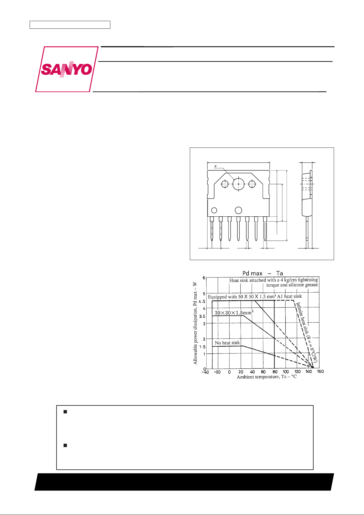
Package Dimensions
unit : mm
3075-SIP7H
Page 2
LA5602
No. 4281-2/5
Parameter Symbol Conditions Ratings Unit
Maximum input voltage V
IN
max 18 V
Enable pin voltage V
EN
max VINmax V
Reset output pin voltage V
RES
max 18 V
Allowable power dissipation Pd max 1.5 W
Operating temperature Topg –30 to +80 °C
Storage temperature Tstg –55 to +150 °C
Specifications
Maximum Ratings at Ta = 25°C
Parameter Symbol Conditions Ratings Unit
Input voltage V
IN
5.6 to 17 V
Output current I
OUT
0 to 350 mA
Reset output source current I
ORH
0 to 200 µA
Reset output synch current I
ORL
0 to 2 mA
Operating Conditions at Ta = 25°C
Parameter Symbol Conditions
Ratings
Unit
min typ max
[Power Supply Section]
Output voltage V
OUT
4.75 5.0 5.25 V
Drop-out voltage V
DROP
0.5 1.0 V
Line regulation ∆V
OLN
5.6≤VIN≤17V 20 100 mV
Load regulation ∆V
OLD
5mA≤IO≤350mA 50 150 mV
Peak output current I
OP
350 500 mA
Output short current I
OSC
100 400 mA
Current dissipation
I
Q
1I
OUT
= 0 2.1 4 mA
I
Q
21050mA
Output noise voltage V
N5
10Hz≤f≤100kHz 70 µVrms
Temperature coefficient of output voltage ∆V
O
/∆Ta Tj = 25 to 125°C 1.6 mV/°C
Ripple rejection Rref f = 120Hz, 6V≤V
IN
≤17V 60 dB
Output on-control voltage V
ENH
2.6 V
Output off-control voltage V
ENL
1.0 V
Low output voltage V
O OFF
0.3 V
[Reset Section]
High reset output voltage V
ORHIORH
= 200µA, Cd pin open 4.73 4.98 5.23 V
Low reset output voltage V
ORLISRL
= 2mA, Cd - GND shorted 100 200 mV
Reset threshold voltage V
RT
3.95 4.2 4.45 V
Reset hysteresis voltage Vhys 50 100 200 mV
Reset output delay time td Cd = 0.1µF 7.5 10 12.5 ms
Operating Characteristics at Ta = 25°C, VIN= 8 V, I
OUT
= 350 mA, C
OUT
= 47µF, according to specified Test Circuit
Page 3

LA5602
No. 4281-3/5
Equivalent Circuit Block Diagram
Specified Test Circuit
Application Circuit Example
Notes: 1) Capacitors Cn and C
RES
are only required if problems are experienced with noise from external sources. If
capacitor Cn is present, ensure that COis at least more than one-third of the value of Cin in order to prevent
output noise at power-down due to capacitor discharge timing.
2) Use a low temperature coefficient capacitor for the delay time capacitor Cd.
3) The minimum recommended value of output capacitor Co is 47µF.
Page 4

LA5602
No. 4281-4/5
Function Table
Reset Operation
Page 5

LA5602
PS No. 4281-5/5
This catalog provides information as of December, 1999. Specifications and information herein are
subject to change without notice.
Specifications of any and all SANYO products described or contained herein stipulate the performance,
characteristics, and functions of the described products in the independent state, and are not guarantees
of the performance, characteristics, and functions of the described products as mounted in the customer’s
products or equipment. To verify symptoms and states that cannot be evaluated in an independent device,
the customer should always evaluate and test devices mounted in the customer’s products or equipment.
SANYO Electric Co., Ltd. strives to supply high-quality high-reliability products. However, any and all
semiconductor products fail with some probability. It is possible that these probabilistic failures could
give rise to accidents or events that could endanger human lives, that could give rise to smoke or fire,
or that could cause damage to other property. When designing equipment, adopt safety measures so
that these kinds of accidents or events cannot occur. Such measures include but are not limited to protective
circuits and error prevention circuits for safe design, redundant design, and structural design.
In the event that any or all SANYO products (including technical data, services) described or contained
herein are controlled under any of applicable local export control laws and regulations, such products must
not be exported without obtaining the export license from the authorities concerned in accordance with the
above law.
No part of this publication may be reproduced or transmitted in any form or by any means, electronic or
mechanical, including photocopying and recording, or any information storage or retrieval system,
or otherwise, without the prior written permission of SANYO Electric Co., Ltd.
Any and all information described or contained herein are subject to change without notice due to
product/technology improvement, etc. When designing equipment, refer to the “Delivery Specification”
for the SANYO product that you intend to use.
Information (including circuit diagrams and circuit parameters) herein is for example only; it is not
guaranteed for volume production. SANYO believes information herein is accurate and reliable, but
no guarantees are made or implied regarding its use or any infringements of intellectual property rights
or other rights of third parties.
 Loading...