

Page 1
Any and all SANYO products described or contained herein do not have specifications that can handle
applications that require extremely high levels of reliability, such as life-support systems, aircraft’s
control systems, or other applications whose failure can be reasonably expected to result in serious
physical and/or material damage. Consult with your SANYO representative nearest you before using
any SANYO products described or contained herein in such applications.
SANYO assumes no responsibility for equipment failures that result from using products at values that
exceed, even momentarily, rated values (such as maximum ratings, operating condition ranges,or other
parameters) listed in products specifications of any and all SANYO products described or contained
herein.
Monolithic Linear IC
Low Saturation Regulator with Reset
Ordering number:ENN3222A
LA5601
SANYO Electric Co.,Ltd. Semiconductor Company
TOKYO OFFICE Tokyo Bldg., 1-10, 1 Chome, Ueno, Taito-ku, TOKYO, 110-8534 JAPAN
Overview
The LA5601 is a voltage regulator with a low-voltage detector and reset controller for use in microprocessor-based
systems. It generates a reset signal for low power supply
voltage. It also features a low 0.25V (typ.) saturation voltage for reduced power dissipation and power supply size.
Applications include microprocessor-controlled consumer
electronic equipment such as CD players, tuners and receivers, and preamplifiers.
Functions
• Low saturation regulator with 250mA and 5.2V output.
• Power supply reset generator function.
• Supports on-off control of 5.2V using equipped enable
pin (high active).
• Built-in Darlington driver (120mA).
• Built-in auxiliary regulator (5.2V, 250mA).
Features
• Low minimum input-output voltage difference (0.3V typ).
• Supports setting of reset output delay time using external
capacitor.
• Built-in fold-back current limiting circuit and excessive
heat protection circuit.
• Reset output using active pull-up for simpler noise reduction and use with internal pull-down logic circuits.
• Error amplifier noise filter pin.
• Auxiliary regulator with reverse current protection.
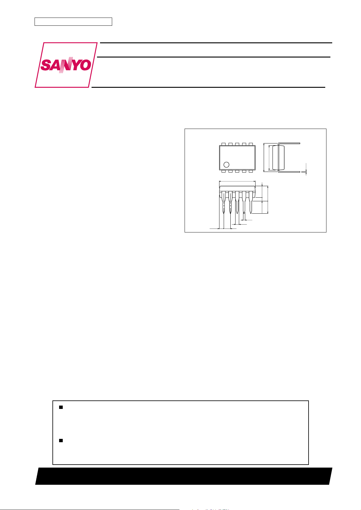
Package Dimensions
unit:mm
3098B-DIP10S
[LA5601]
10
1
1.14 1.78
6
5
9.4
0.48
0.95
7.62
3.0
3.9max
3.2
0.51min
6.4
0.25
SANYO : DIP10S
40500TN (KT)/92595HA/D059TA, TS (US) No.3222–1/8
Page 2
Specifications
Absolute Maximum Ratings at Ta = 25˚C
retemaraPlobmySsnoitidnoCsgnitaRtinU
egatlovtupnIV
egatlovnipelbanEV
egatlovniptuptuoteseRV
egatlovtuptuorevirDV
egatlovtupnirevirDV
noitapissidrewopelbawollAxamdP 1W
erutarepmetgnitarepOrpoT 08+ot03–
erutarepmetegarotSgtsT 051+ot55–
Operating Conditions at Ta = 25˚C
retemaraPlobmySsnoitidnoCsgnitaRtinU
egatlovtupnIV
tnerructuptuOI
tnerructuptuoteserlevel-HI
tnerructuptuoteserlevel-LI
tnerructuptuorotalugeryrailixuAI
egatlovtuptuorevirDV
tnerructuptuorevirdlevel-LI
egatlovtupnirevirdlevel-HV
egatlovtupnirevirdlevel-LV
Operating Characteristics at Tj = 25˚C, VIN=6V, I
retemaraPlobmySsnoitidnoC
V,etats-NOtuptuO:rotalugerniaM[
egatlovtuptuOV
egatlovtuoporDV
noitalugereniL
noitalugerdaoL
tnerructuptuokaePI
tnerructrohstuptuOI
niardtnerruC
egatlovesiontuptuOV
noitcejerelppiRjerRV7,zH021=f ≤VNI≤ V3147Bd
egatlovtuptuolevel-LV
tnerructnecseiuQI
]tiucricteseR[
egatlovtuptuoteserlevel-HV
egatlovtuptuoteserlevel-LV
egatlovdlohserhtteseRV
egatlovsiseretsyhteseRsyhVI
emityaledtuptuoteseRt
]rotalugeryrailixuA[
egatlovtuptuOV
noitalugereniL
noitalugerdaoL
tnerructrohstuptuOI
tnerrucegakaelniptuptuOI
]revirdnotgnilraD[
egatlovtuptuorevirdlevel-L
tnerructupnirevirdlevel-HI
tnerrucegakaelniptuptuOI
NE
egatlovtuptuofotneiciffeocerutarepmeT
egatlovlortnocetats-NOtuptuOV
V,etats-FFOtuptuO:rotalugerniaM[
]'L'=
NE
egatlovlortnocetats-FFOtuptuOV
xam 51V
NI
xam VNIxamV
NE
xam 51V
SER
xam 51V
DO
xam 51V
DI
NI
TUO
HRO
LRO
AO
xam 41V
DO
xam 021Am
LDO
I
HDI
I
LDI
]neporo'H'=
O
I
PORD
∆V
1
V5.5 ≤VNI≤ V410308Vm
NLO
∆V
2
V6 ≤VNI≤ V410204Vm
NLO
∆V
1
Am5 ≤I
DLO
∆V
2
Am5 ≤I
DLO
PO
CSO
IQ1I
IQ2 0103Am
ON
∆VO/∆ jT
∆V
∆V
V
V
Tj=25 to 80°C
HNE
VNE0=05002Vm
FFOO
VNE0=5.14Am
FFOQ
LNE
I
HRO
I
LRO
I
TR
d
I
AO
AO
V6 ≤VNI≤ I,V41
NLAO
Am2 ≤IAO≤ Am01031002Vm
DLAO
CSAO
VNIV,0=
KAELAO
1I
LDO
2I
LDO
I
HDI
V
HDO
HI
LA5601
˚C
˚C
41ot9.5V
052ot0Am
002ot0Aµ
2ot0Am
01ot0Am
Am021= 41ot3V
LDO
≤ Aµ0013.0+ot3.0–V
LDO
=200mA, See specified Test Circuit.
OUT
sgnitaR
nimpytxam
0.52.54.5V
Am052=52.05.0V
TUO
≤ Am05204001Vm
TUO
≤ Am0014105Vm
TUO
0=2.26Am
TUO
zH01 ≤f≤ zHk00107smrVµ
NOrevird,rotalugerniaM6.2V
FFOrevird,rotalugerniaM 0.1V
Aµ002=79.471.573.5V
HRO
V,Am2=
LRO
Am5=7.39.31.4V
TUO
Am5=05051003Vm
TUO
Fµ1.0=dC5.7015.21sm
Am5=2.34.36.3V
AO
LDO
LDO
LDO
V,V41=
V7.3=09002Vm
NI
Am5=5104Vm
AO
V6=2Aµ
V,Am08=
V3=1.16.1V
DI
V,Am021=
V3=2.18.1V
DI
V,Am021=
V3=4.01Am
DI
V,V41=
DO
V3.0=05Aµ
DI
052005Am
08003Am
7.0–
0103Am
No.3222–2/8
tinU
mV/˚C
V
NI
Page 3
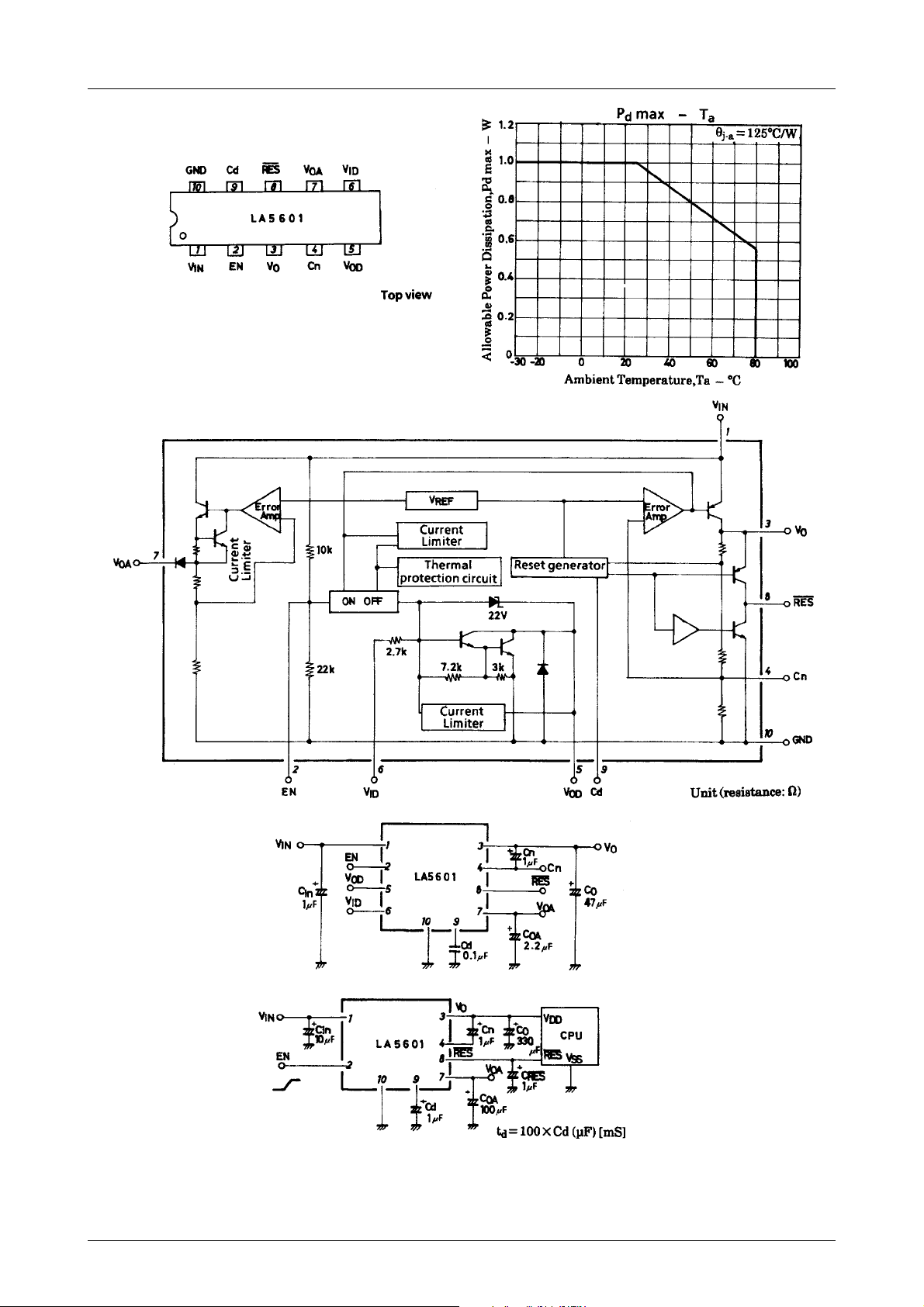
Pin Assignment
Equivalent Circuit Block Diagram
LA5601
Specified Test Circuit
Sample Application Circuit 1
Note ) 1. Capacitors Cn and C
external sources.
2. If capacitor Cn is present, ensure that Co is at least more than one-third of the value of C
in order to prevent output noise at power-down due to capacitor discharge timing.
3. The minimum recommended value of output capacitor Co is 47µF.
4. Use low temperature coefficient capacitor for the delay time capacitor Cd.
are only required if problems are experienced with noise from
RES
in
No.3222–3/8
Page 4

Function Table
V
NE
LL FFO
HH NO
V
O
VEN=’H’ or open.
Reset Operation
LA5601
revirD
Enable Circuit
Sample Application Circuit 2
(Delay start regulator)
Sample Application Circuit 3
(Positive-to-negative DC converter)
Note ) 1. The output voltage can be fine-trimmed by adjusting R1. To protect the output transistor
against overvoltage, ensure that either R1 is non zero or use a low-Q coil for L1.
2. A load must always be present on power-up. To safeguard against excessive output voltages
that occur when the circuit is powered up without a load, a dummy load resistor is recommended. This is shown on the circuit as R2.
3. Select VIN, R1 and L1 so that VOD<14V, and I
reguire that VIN never exceeds 9V.
<120mA. The component values shown
ODL
No.3222–4/8
Page 5

LA5601
No.3222–5/8
Page 6

LA5601
No.3222–6/8
Page 7

LA5601
No.3222–7/8
Page 8

LA5601
Specifications of any and all SANYO products described or contained herein stipulate the performance,
characteristics, and functions of the described products in the independent state, and are not guarantees
of the performance, characteristics, and functions of the described products as mounted in the customer's
products or equipment. To verify symptoms and states that cannot be evaluated in an independent device,
the customer should always evaluate and test devices mounted in the customer's products or equipment.
SANYO Electric Co., Ltd. strives to supply high-quality high-reliability products. However, any and all
semiconductor products fail with some probability. It is possible that these probabilistic failures could
give rise to accidents or events that could endanger human lives, that could give rise to smoke or fire,
or that could cause damage to other property. When designing equipment, adopt safety measures so
that these kinds of accidents or events cannot occur. Such measures include but are not limited to protective
circuits and error prevention circuits for safe design, redundant design, and structural design.
In the event that any or all SANYO products(including technical data,services) described or
contained herein are controlled under any of applicable local export control laws and regulations,
such products must not be exported without obtaining the export license from the authorities
concerned in accordance with the above law.
No part of this publication may be reproduced or transmitted in any form or by any means, electronic or
mechanical, including photocopying and recording, or any information storage or retrieval system,
or otherwise, without the prior written permission of SANYO Electric Co. , Ltd.
Any and all information described or contained herein are subject to change without notice due to
product/technology improvement, etc. When designing equipment, refer to the "Delivery Specification"
for the SANYO product that you intend to use.
Information (including circuit diagrams and circuit parameters) herein is for example only ; it is not
guaranteed for volume production. SANYO believes information herein is accurate and reliable, but
no guarantees are made or implied regarding its use or any infringements of intellectual property rights
or other rights of third parties.
This catalog provides information as of April, 2000. Specifications and information herein are subject to
change without notice.
PS No.3222–8/8
 Loading...