

SANYO LA5318V Datasheet

Overview
The LA5318V is a variable voltage-dividing voltage
generator IC designed for driving LCD matrixes that
require multiple voltages.
Package Dimensions
unit: mm
3179A-SSOP20
Monolithic Linear IC
Ordering number : EN5670
82097HA(OT) No. 5670-1/4
SANYO: SSOP20
[LA5318V]
SANYO Electric Co.,Ltd. Semiconductor Bussiness Headquarters
TOKYO OFFICE Tokyo Bldg., 1-10, 1 Chome, Ueno, Taito-ku, TOKYO, 110 JAPAN
Voltage-Dividing Voltage Generator
for Multi-Voltage LCD Matrix Drive
LA5318V
Parameter Symbol Conditions Ratings Unit
Maximum supply voltage V
EE
max V
CC
– V
EE
36 V
Maximum output current I
OUT
max V1 to V4 Internal* mA
Allowable power dissipation Pd max 330 mW
Operating temperature Topr –20 to +75 °C
Storage temperature Tstg –30 to +125 °C
Specifications
Absolute Maximum Ratings at Ta = 25°C
Parameter Symbol Conditions Ratings Unit
Supply voltage V
EE
V
CC
– V
EE
–35.5 to –6 V
Input voltage V
REF
V
CC
– V
REF
: V
REF
≥ V
EE
–35 to –6 V
Input current I
INR
INR –0.2 to 0 mA
I
OUTR
OUTR 0 to 50 mA
Output current I
OUT
1, 2 V1, V2 –5 to +5 mA
I
OUT
3,4 V3, V4 –10 to +5 mA
Operating Conditions at Ta = 25°C
Notes: *The value stipulated in the conditions listed in the separate document shall be used as the maximum output current.
1. Continuous operation (without damage to the device) is guaranteed in the above ranges.
2. The output pins V1 to V4 may be shorted to the power supply or to ground for periods of up to 1 ms. (When |V
CC
– VEE| < 35 V)
Note: VCCand VEEmust be set up so that |V1| and |VEE– V4| are at least 1 V.
Allowable power dissipation, Pd – mW
Ambient temperature, Ta – °C
No. 5670-2/4
LA5318V
Parameter Symbol Conditions
Ratings
Unit
min typ max
Current drain I
CC
, IEEVCC– VEE= –20 V, RX= 8R, INR = VCC: VCC, V
EE
0.35 0.5 mA
Output voltage ratio 1 Ra1 V2/V1 1.96 2.00 2.04
Output voltage ratio 2 Ra2 (V
REF
– V3)/(V
REF
– V4) 1.96 2.00 2.04
Output voltage ratio 3 Rb1 V
REF
/V1 11.64 12.00 12.36
Output voltage ratio 4 Rb2 V
REF
/V2 5.82 6.00 6.18
Output voltage ratio 5 Rb3 V
REF
/(V
REF
– V3) 5.82 6.00 6.18
Output voltage ratio 3 Rb4 V
REF
/(V
REF
– V4) 11.64 12.00 12.36
Internal resistance ratio 1 R
X
1 RX1 – RX2 8
Internal resistance ratio 2 R
X
2 RX1 – RX3
Referenced to the resistance
12
Internal resistance ratio 3 R
X
3 RX1 – RX4
R between R
X
4 and VIN3
14
Internal resistance ratio 4 R
X
4 RX1 – VIN3 15
Resistance R
The value of R when the voltage across
30 kΩ
R
X
4 and VIN3 is 0.5 V.
Load regulation 1 ∆V1 +0.1 mA < I
OUT
1 < +5 mA : V1 ±20 mV
Load regulation 2 ∆V2 +0.1 mA < I
OUT
2 < +5 mA : V2 ±20 mV
Load regulation 3 ∆V3 +0.1 mA < I
OUT
3 < +5 mA : V3 ±20 mV
Load regulation 4 ∆V4 +0.1 mA < I
OUT
4 < +5 mA : V4 ±20 mV
Load regulation –1A –∆V1A –0.5 mA < I
OUT
1 < –0.1 mA : V1 ±20 mV
Load regulation –2A –∆V2A –0.5 mA < I
OUT
2 < –0.1 mA : V2 ±20 mV
Load regulation –3 –∆V3 –10 mA < I
OUT
3 < –0.1 mA : V3 ±20 mV
Load regulation –4 –∆V4 –10 mA < I
OUT
4 < –0.1 mA : V4 ±20 mV
Load regulation –1B –∆V1B –5 mA < I
OUT
1 < –0.1 mA, BIN= GND : V1 ±20 mV
Load regulation –2B –∆V2B –5 mA < I
OUT
2 < –0.1 mA, BIN= GND : V2 ±20 mV
OUTR pin saturation voltage V
OUTRIOUT
= 20 mA, VCC– INR = 2.7 : OUTR – V
EE
0.5 V
Operating Characteristics at Ta = 25°C, VCC–VEE= –20 V, V
REF
= VEE, RX= 8R, BIN= OPEN
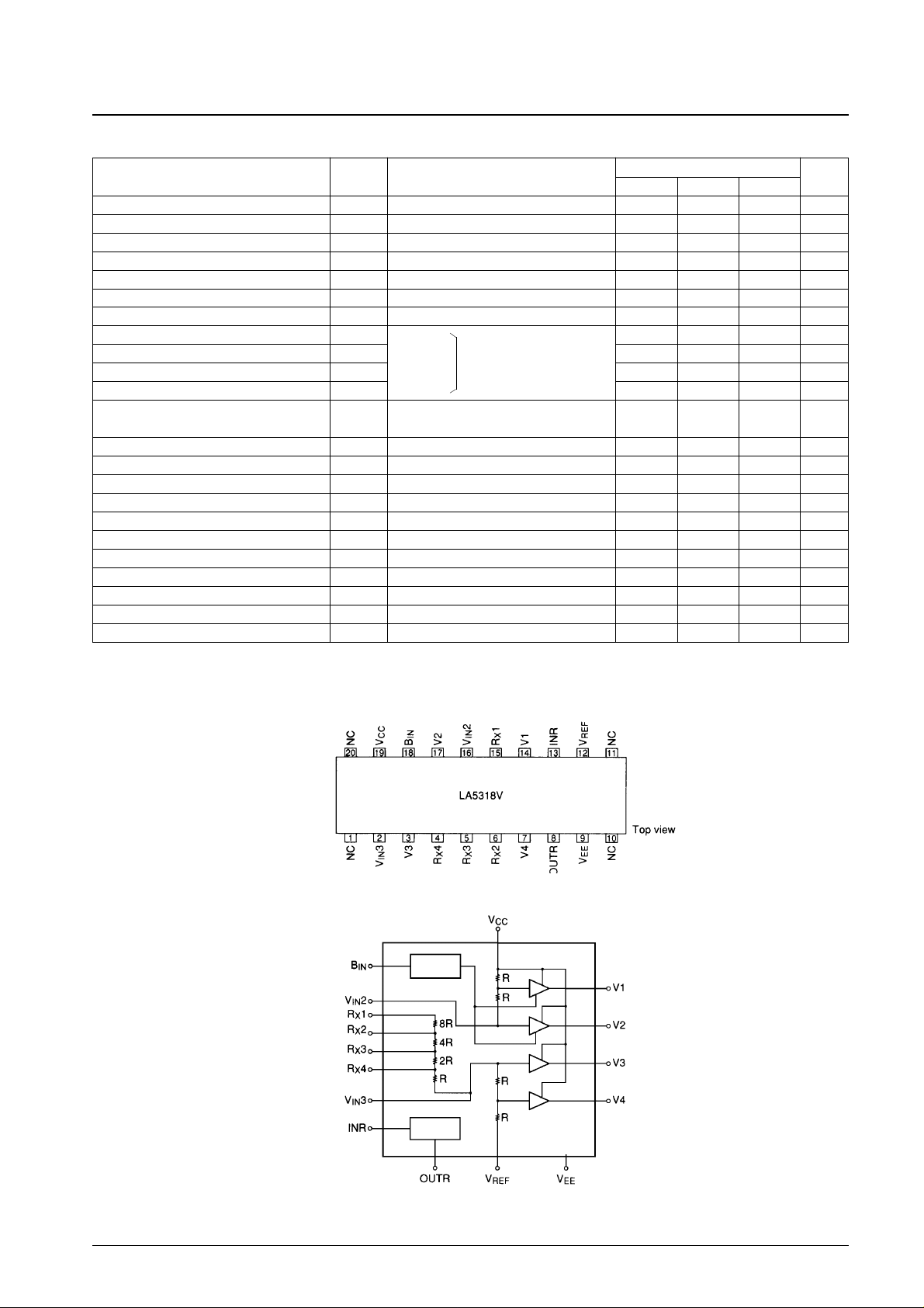
Pin Assignment
Block Diagram
(This circuit must be used with VRX1 ≥ VRX2 ≥ VRX3 ≥ VRX4.)
V1, V2 bias
control
V
REF
control
Note: For I
OUT
, minus (–) indicates source current and plus (+) indicates sink current.
 Loading...