

Page 1
Any and all SANYO products described or contained herein do not have specifications that can handle
applications that require extremely high levels of reliability, such as life-support systems, aircraft’s
control systems, or other applications whose failure can be reasonably expected to result in serious
physical and/or material damage. Consult with your SANYO representative nearest you before using
any SANYO products described or contained herein in such applications.
SANYO assumes no responsibility for equipment failures that result from using products at values that
exceed, even momentarily, rated values (such as maximum ratings, operating condition ranges,or other
parameters) listed in products specifications of any and all SANYO products described or contained
herein.
Monolithic Linear IC
Variable Divided Voltage Generator
for LCD Use
Ordering number:ENN4145
LA5318M
SANYO Electric Co.,Ltd. Semiconductor Company
TOKYO OFFICE Tokyo Bldg., 1-10, 1 Chome, Ueno, Taito-ku, TOKYO, 110-8534 JAPAN
Overview
The LA5318M is a variable divided voltage generator IC
for multiple drive of LCD matrix.
Features
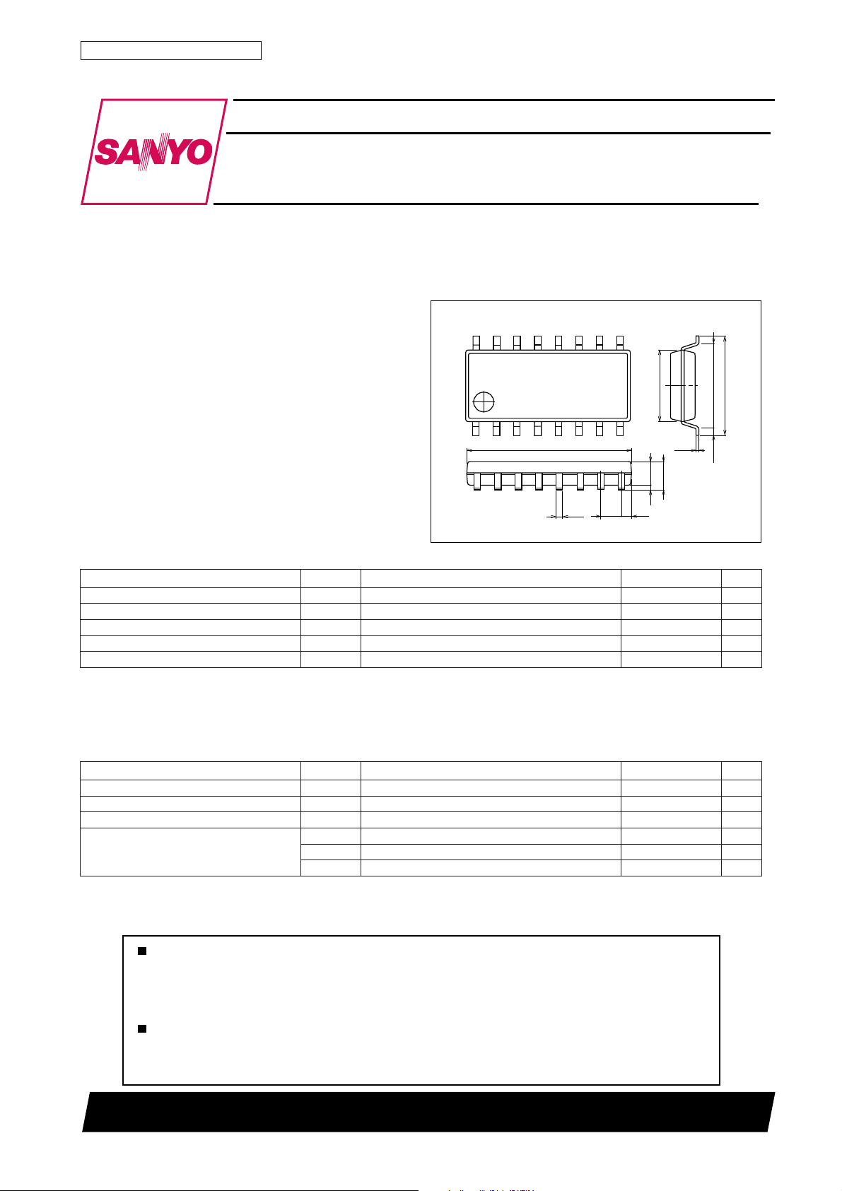
Package Dimensions
unit:mm
3035A-MFP16
16
[LA5318M]
• Power supply for variable bias LCD division drive (1/5
to 1/19 bias available by built-in resistances).
• Four operational amplifiers to deliver 5 voltage outputs.
• Low current drain (0.35mA typ).
• V1, V2 output current source side variable pin.
• Output on/off function V
• Miniflat package.
control pins.
REF
1
10.1
0.35
Specifications
Absolute Maximum Ratings at Ta = 25˚C
retemaraPlobmySsnoitidnoCsgnitaRtinU
egatlovylppusmumixaMV
tnerructuptuomumixaMI
noitapissidrewopelbawollAxamdP 033Wm
erutarepmetgnitarepOrpoT 57+ot02–
erutarepmetegarotSgtsT 531+ot03–
Note : 1. Continuous operation (nonbreakdown) is guaranteed when operated at the maximum ratings shown above.
2. *The maximum output current is a value specified under the conditions otherwise specified separately.
3. Output pins V1 to V4 to VCC, GND short circuit not lasting more than 1ms is acceptable (| VCC – VEE | < 35V).
xamVCCV-
EE
xam4Vot1V *lanretnIAm
TUO
EE
1.27
9
4.4
8
0.15
1.5
1.8max
0.1
0.605
SANYO : MFP16
6.4
5.15
0.625
63V
˚C
˚C
Operating Conditions at Ta = 25˚C
retemaraPlobmySsnoitidnoCsgnitaRtinU
egatlovylppuSV
egatlovtupnIV
tnerructupnII
I
tnerructuptuO
Note : 4. Set VCC and VEE so that | V1 | and | VEE-V4 | become 1V or greater.
I
I
V
EE
FER
RNI
RTUO
2,1TUO
4,3TUO
≥ V
FER
EE
31500TN (KT)/53196RM No.4145–1/5
6–ot5.53–V
6–ot53–V
0ot2.0–Am
05+ot0Am
5+ot5–Am
5+ot01–Am
Page 2
LA5318M
Operating Characteristics at Ta = 25˚C, VCC–VEE=20V, V
retemaraPlobmySsnoitidnoC
niardtnerruCI
1oitaregatlovtuptuO1aR1V/2V69.100.240.2
2oitaregatlovtuptuO2aRV(
3oitaregatlovtuptuO1bRV
4oitaregatlovtuptuO2bRV
5oitaregatlovtuptuO3bRV
6oitaregatlovtuptuO4bRV
1oitarecnatsiserlanretnIR
2oitarecnatsiserlanretnIR
3oitarecnatsiserlanretnIR
4oitarecnatsiserlanretnIR
ecnatsiseRRRssorcadeilppasiV5.0nehweulavR
1noitalugerdaoL
2noitalugerdaoL
3noitalugerdaoL
4noitalugerdaoL
A1–noitalugerdaoL–∆ A1VI<Am5.0–
A2–noitalugerdaoL–∆ A2VI<Am5.0–
3–noitalugerdaoL–∆ 3VI<Am01–
4–noitalugerdaoL–∆ 4VI<Am01–
B1–noitalugerdaoL–∆ B1VI<Am5–
B2–noitalugerdaoL–∆ B2VI<Am5–
egatlovnoitarutasRTUOV
CCI,EE
∆ 1V
∆ 2V
∆ 3V
∆ 4V
VCCV–
EE
V(/)3V-
FER
1V/46.1100.2163.21
FER
2V/28.500.681.6
FER
V(/
FER
FER
V(/
FER
1RXR-1X*28
X
2RXR-2X*321
X
3RXR-3X*441
X
4RXV-4
X
I
RTUO
FER
*351
NI
I<Am1.0+
TUO
I<Am1.0+
TUO
I<Am1.0+
TUO
I<Am1.0+
TUO
TUO
TUO
TUO
TUO
TUO
TUO
TUO
V,Am02=
Note* : Referenced to R between RX4 and VIN3.
REF=VEE
R,V02=
X
FER
)3V-28.500.681.6
)4V-46.1100.2163.21
CC
, RX=8R, BIN=Open
sgnitaR
nimpytxam
V=RNI,R8=
CC
)4V-69.100.240.2
Vdna4
Am5+<102±Vm
Am5+<202±Vm
Am5+<302±Vm
Am5+<402±Vm
Am1.0–<102±Vm
Am1.0–<202±Vm
Am1.0–<302±Vm
Am1.0–<402±Vm
B,Am1.0–<1
NI
B,Am1.0–<2
NI
I.knisdna)–(evitagen
TUO
X
DNG=02±Vm
DNG=02±Vm
IecruoS(V7.2=RNI–
303kΩ
NI
si
TUO
).)+(evitisopsi
53.05.0Am
tinU
5.0V
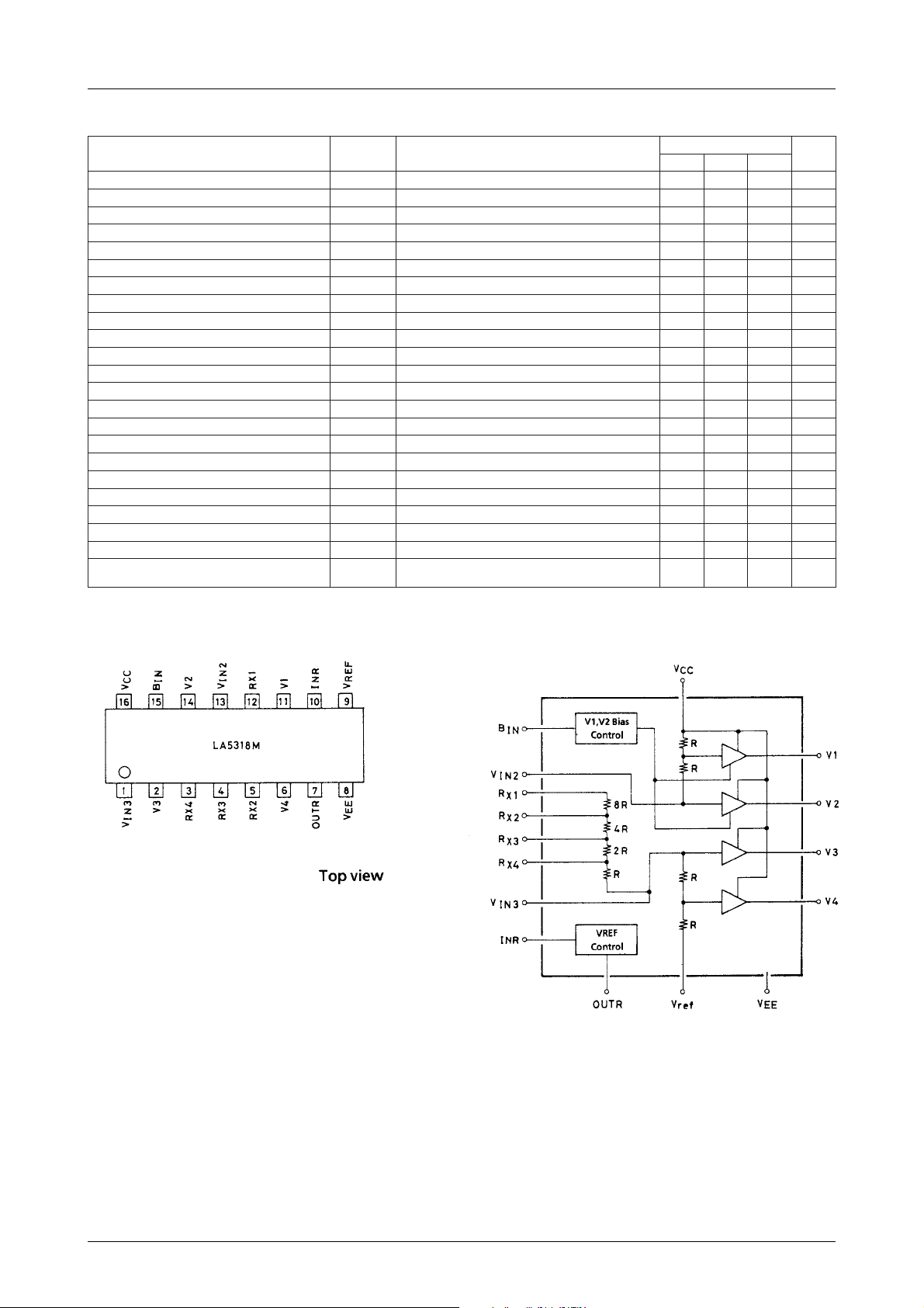
Pin Assignment Block Diagram
Note : Use the IC so that V
must be obeyed.
RX1≥VRX2≥VRX3≥VRX4
No.4145–2/5
Page 3

LA5318M
Maximum Output Current Load Test Conditions
VCC–VEE=35V RX=8R C1 to C4=10µF C5=33µF R ; 1W or more
Q1 to 4 ; 2SA984 E or F rank
Q5 to 9 ; 2SC2274 E or F rank
Output load resistances R1 to R8 are set in order that current of 25 to 30mA max. (V3, V4 source side : about 60mA) are
supplied to both source and sink sides when an on-level input is applied to the inputs 1 or 2.
V
Control Block
REF
How to calculate the Q1 drive current.
VCC – VBE – V
I=
11k + R
IN
(VBE≈0.7V)
Drive current
IO≈10I= ×10
VCC – 0.7 – V
11k + R
IN
Q1 hFE is assumed to be 50.
* Set VCC=INR when INR and OUTR are not used.
No.4145–3/5
Page 4

LA5318M
No.4145–4/5
Page 5

LA5318M
Specifications of any and all SANYO products described or contained herein stipulate the performance,
characteristics, and functions of the described products in the independent state, and are not guarantees
of the performance, characteristics, and functions of the described products as mounted in the customer's
products or equipment. To verify symptoms and states that cannot be evaluated in an independent device,
the customer should always evaluate and test devices mounted in the customer's products or equipment.
SANYO Electric Co., Ltd. strives to supply high-quality high-reliability products. However, any and all
semiconductor products fail with some probability. It is possible that these probabilistic failures could
give rise to accidents or events that could endanger human lives, that could give rise to smoke or fire,
or that could cause damage to other property. When designing equipment, adopt safety measures so
that these kinds of accidents or events cannot occur. Such measures include but are not limited to protective
circuits and error prevention circuits for safe design, redundant design, and structural design.
In the event that any or all SANYO products(including technical data,services) described or
contained herein are controlled under any of applicable local export control laws and regulations,
such products must not be exported without obtaining the export license from the authorities
concerned in accordance with the above law.
No part of this publication may be reproduced or transmitted in any form or by any means, electronic or
mechanical, including photocopying and recording, or any information storage or retrieval system,
or otherwise, without the prior written permission of SANYO Electric Co. , Ltd.
Any and all information described or contained herein are subject to change without notice due to
product/technology improvement, etc. When designing equipment, refer to the "Delivery Specification"
for the SANYO product that you intend to use.
Information (including circuit diagrams and circuit parameters) herein is for example only ; it is not
guaranteed for volume production. SANYO believes information herein is accurate and reliable, but
no guarantees are made or implied regarding its use or any infringements of intellectual property rights
or other rights of third parties.
This catalog provides information as of March, 2000. Specifications and information herein are subject to
change without notice.
PS No.4145–5/5
 Loading...