

SANYO LA5314 Datasheet
Ordering number: EN5376
Monolithic Linear IC
LA5314
Variable Divided Voltage Generator
for LCD Use
Overview
The LA5314 is a valiable diveded voltage generator IC for
multiple drive of LCD matrix.
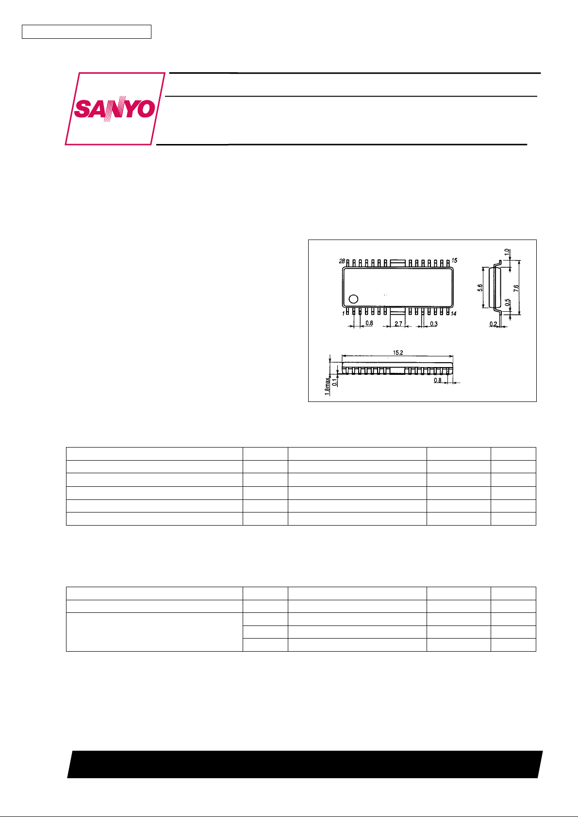
Package Dimensions
unit : mm
3222-HSOP28
[LA5314]
Features
.
Power supply for variable bias LCD matrix. (1/5 to 1/20 bias
available by built-in resistances)
.
Five operational amplifiers to deliver 5 voltage outputs
.
Low current drain (1.6 mA typ)
.
Miniflat package for miniturization
SANYO : HSOP28
Specifications
Maximum Ratings atTa=25°C
Parameter Symbol Conditions Ratings Unit
Maximum supply voltage V
Maximum output current l
Allowable power dissipation Pd max 600 mW
Operating temperature Topr –20 to +75 °C
Storage temperature Tstg –30 to +150 °C
max VCC–V
CC
max V0 to V4
OUT
EE
38 V
*±25
mA
Note: 1. Continuous operation (non breakdown) is guaranteed when operated at the maximum ratings shown above.
2. *The maximum output current is a value specified under the conditions otherwise specified separately.
Operating Conditions at Ta = 25°C
Parameter Symbol Conditions Ratings Unit
Supply voltage V
l
OUT
Output current
Note: 3. Set VCCand VEEso that |V0–V1| and |V4| become 1V or greater.
l
OUT
l
OUT
VCC–V
CC
0, 1 V0, V1 –0.5 to +10 mA
2, 3 V2, V3 –10 to +10 mA
4 V4 –15 to +0.5 mA
EE
10 to 35 V
SANYO Electric Co.,Ltd. Semiconductor Bussiness Headquarters
TOKYO OFFICE Tokyo Bldg., 1-10, 1 Chome, Ueno, Taito-ku, TOKYO, 110 JAPAN
83096HA(II) No.5376-1/5
LA5314
Operating Chararcteristics at Ta = 25°C, VCC– VEE= 20 V, V
Parameter Symbol Conditions min typ max Unit
Current drain I
Output voltage difference 1 Vd1 (V0 – V1) – (V1 – V2) –30 +30 mV
Output voltage difference 2 Vd2 (V3 – V4) – (V4 – V
Output voltage ratio 1 Rb1 V0/(V0 – V1) 11.64 12.00 12.36 —
Output voltage ratio 2 Rb2 V0/(V0 – V2) 5.82 6.00 6.18 —
Output voltage ratio 3 Rb3 V0/V3 5.82 6.00 6.18 —
Output voltage ratio 4 Rb4 V0/V4 11.64 12.00 12.36 —
Internal resistnace ratio 1 8R R
Internal resistance ratio 2 12R R
Internal resistance ratio 3 14R R
Internal resistance ratio 4 15R R
Resistance R
Load regulation 1 ∆V0 V0: –0.2 mA < I
Load regulation 2 ∆V1 V1: –0.2 mA < I
Load regulation 3 ∆V2 V2: –10.0 mA < I
Load regulation 4 ∆V3 V3: –10.0 mA < I
Load regulation 5 ∆V4 V4: –10.0 mA < I
CC,IEE
VCC,VEE:VCC–VEE=20V,RX= 8R 1.6 3 mA
) –30 +30 mV
EE
1–RX2* 8—
X
1–RX3* 12 —
X
1–RX4* 14 —
X
1–VIN3* 15 —
X
R value when 0.6 V is applied across R
R
5–RX6
X
0 < +10.0 mA –20 +20 mV
OUT
1 < +10.0 mA –20 +20 mV
OUT
2 < +10.0 mA –20 +20 mV
OUT
3 < +10.0 mA –20 +20 mV
OUT
4 < +0.2 mA –20 +20 mV
OUT
= VCC, RX= 8R
REF
5–RX6:
X
20 kΩ
Note* : Referenced to R between RX4 and VIN3
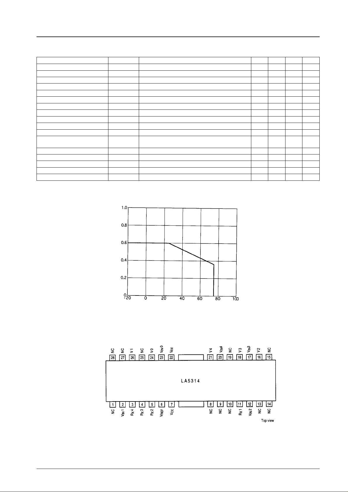
Pd max — Ta
Pin Assignment
Allowable power dissipation, Pd max — W
Temperature, Ta —°C
T00025
No.5376-2/5
 Loading...