

SANYO LA4906 Datasheet
Overview
The LA4906 is a BTL two-channel power amplifier for
use in car audio systems. It uses a signal-following
switching technique in the power supply for the amplifier
output stage and a newly-developed nonlinear amplifier
that features nonlinear characteristics in the signal system.
These features hold increases in the number of external
components to a minimum, and reduce power dissipation
(and thus heat generation) in the practical operating region
to about 1/2 that of earlier class B amplifier ICs. This can
contribute significantly to miniaturization and weight
reduction in the heat sink and to reduction of the heat
generated within the end product case.
Features
• Power dissipation reduced by 50% (for music at average
power levels, as compared to earlier Sanyo products)
• The number of required signal-following switching
circuits has been reduced to just one circuit for two
channels, reducing the number of external components.
• The output is a pure analog signal; no switching noise
whatsoever appears on the output lines.
• Uses a single-voltage power supply from 8 to 18 V.
• Provides a full range of built-in protection circuits,
including shorting of output pin to VCC, shorting of
output pin to ground, overvoltage, and thermal
shutdown protection.
• Built-in standby switch
• Clipping detection function
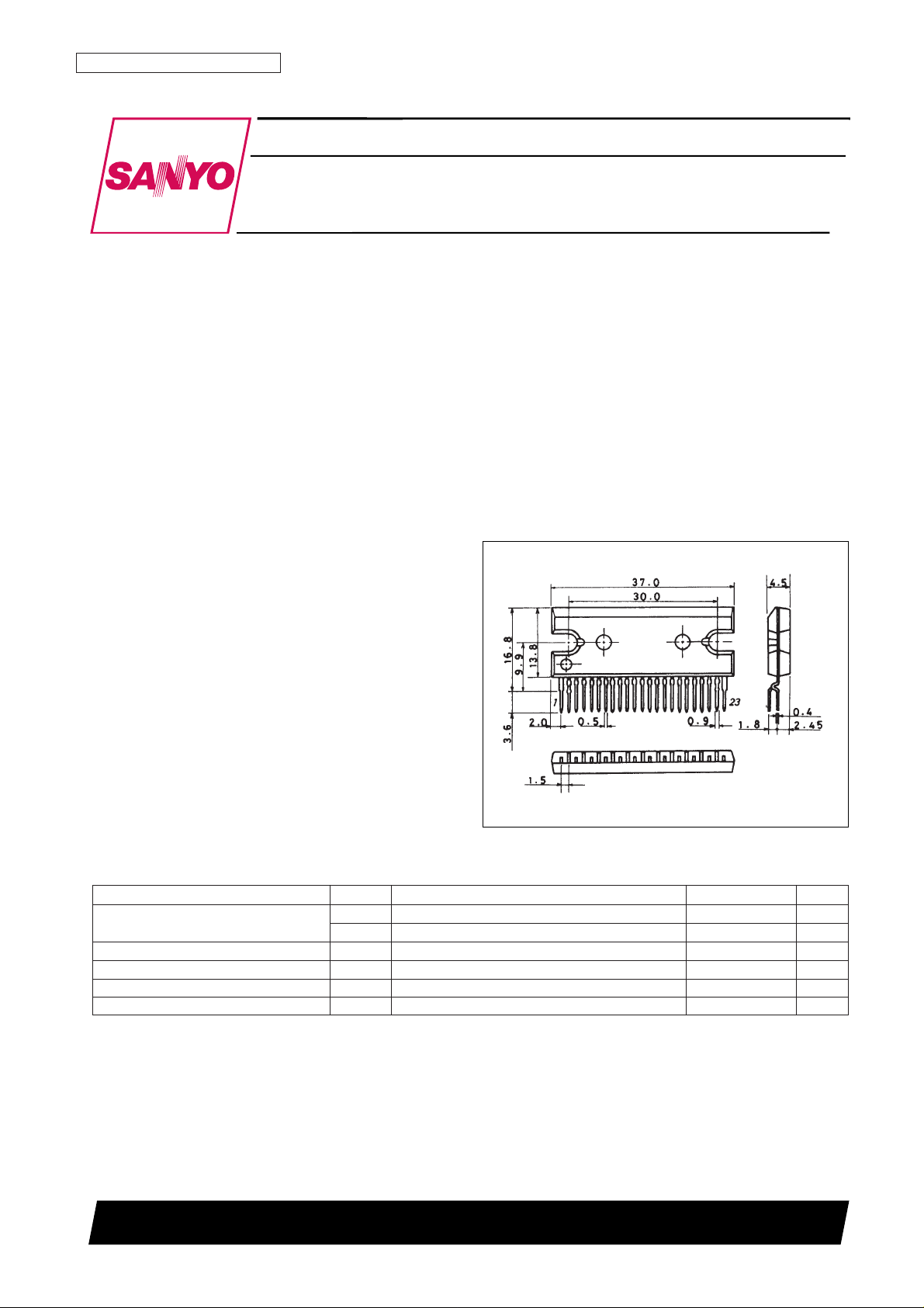
Package Dimensions
unit: mm
3160-SIP23HZ
Monolithic Linear IC
Ordering number : EN *5714
73097HA(OT) No. 5714-1/10
Preliminary
SANYO: SIP23HZ
[LA4906]
SANYO Electric Co.,Ltd. Semiconductor Bussiness Headquarters
TOKYO OFFICE Tokyo Bldg., 1-10, 1 Chome, Ueno, Taito-ku, TOKYO, 110 JAPAN
17-W, 2-Channel BTL AF High-Efficiency
Power Amplifier for Car Audio Systems
LA4906
Parameter Symbol Conditions Ratings Unit
Maximum supply voltage
V
CC
max1 With no signal, t = 1 minute 18 V
V
CC
max2 16 V
Maximum output current I
O
Peak Per channel 4.5 A
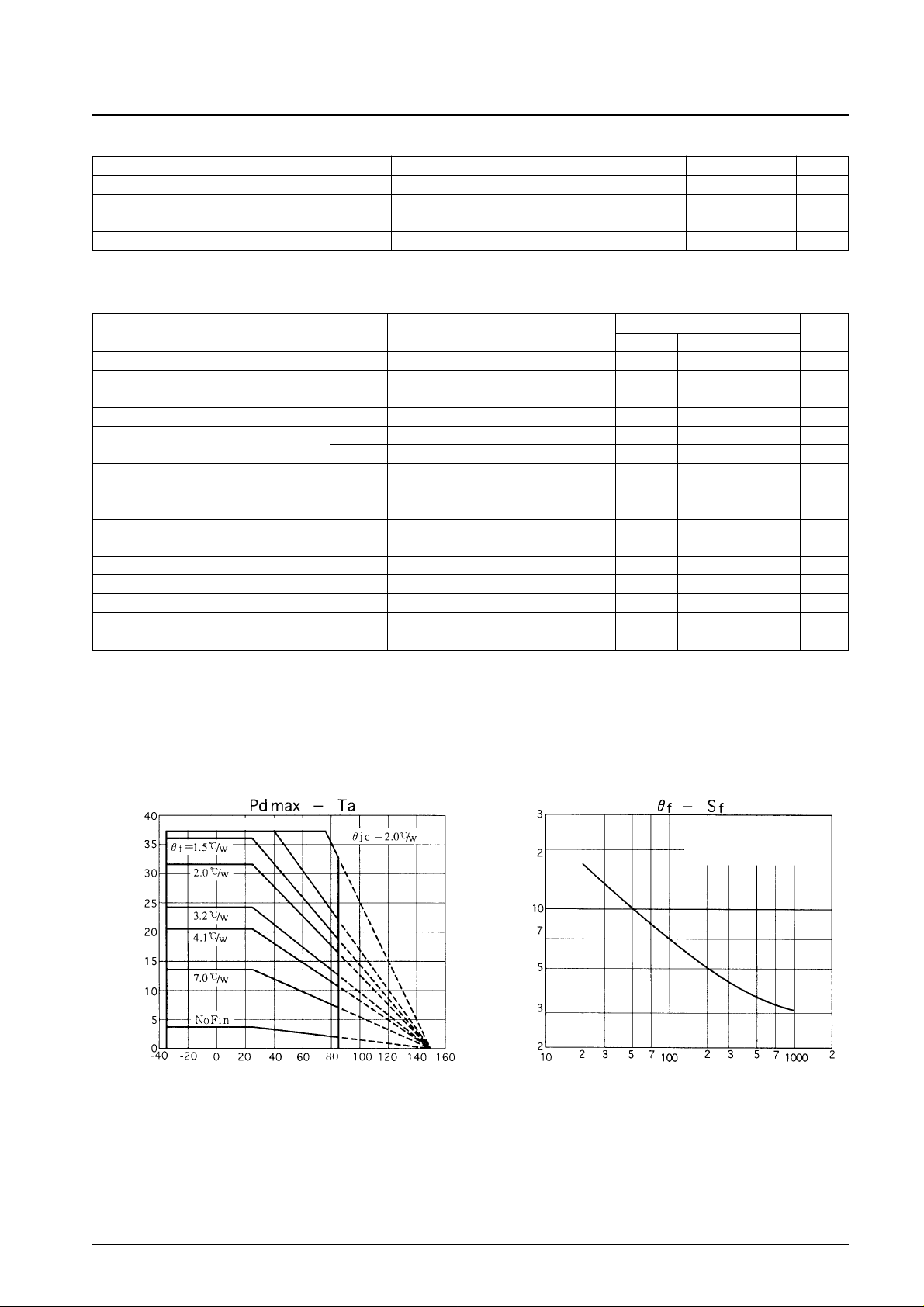
Allowable power dissipation Pd max With an arbitrarily large heat sink 37.5 W
Operating temperature Topr –35 to +85 °C
Storage temperature Tstg –40 to +150 °C
Specifications
Absolute Maximum Ratings at Ta = 25°C
Notes: 1. Set VCCand RLto be in the range where Pd max does not exceed 37.5 W.
2. The overvoltage protection circuit operates at V
CC
= 26 V or higher.
No. 5714-2/10
LA4906
Parameter Symbol Conditions
Ratings
Unit
min typ max
Quiescent current drain I
CC
0 RL= ∞, VIN= 0 80 110 150 mA
Standby current Ist 0 10 µA
Voltage gain VG V
O
= 0 dBm 28 30 32 dB
Total harmonic distortion THD P
O
= 1 W, LPF = 30 kHz 0.07 0.2 %
Output power
P
O
1 THD = 10 %, RL = 4 Ω 14 17 W
P
O
2 THD = 10 %, RL = 2 Ω 25 W
Output noise voltage V
NO
Rg = 0, BPF = 20 Hz to 20 kHz 0.10 0.3 mVrms
Ripple rejection ratio SVRR
Rg = 0, V
CCR
= 0 dBm,
60 75 dB
BPF = 20 Hz to 20 kHz
Channel separation CH sep
Rg = 10 kΩ, V
O
= 0 dBm,
45 60 dB
BPF = 20 Hz to 20 kHz
Input resistance Ri 21 30 39 kΩ
Output offset voltage VN offset Rg = 0 –200 +200 mV
Standby on voltage V
STH
AMP = on, applied through a 10 kΩ resistor 3 V
CC
V
Clipping detect off current I
DOFF
THD = 1 % 1 10 µA
Clipping detect on current I
DON
THD = 10 % 100 150 200 µA
Operating Characteristics
at Ta = 25°C, VCC= 13.2 V, RL= 4 Ω, f = 1 kHz, RG = 600 Ω, in the recommended circuit
Parameter Symbol Conditions Ratings Unit
Recommended supply voltage V
CC
13.2 V
Allowable operating voltage range V
CC
op 8 to 16 V
Recommended load resistance R
L
4 Ω
Recommended load resistance range R
L
op 2 to 4 Ω
Operating Conditions at Ta = 25°C
Note: Set VCCand RLto be in the range where Pd max does not exceed 37.5 W.
Allowable power dissipation, Pd max – W
Heat sink thermal resistance,
θf – °C/W
Heat sink area, Sf – cm
2
Ambient temperature, Ta – °C
With an arbitrarily large heat sink
Al heat sink, t = 1.5 mm
Tightening torque: 39 N·cm
With silicone grease applied.
No. 5714-3/10
LA4906
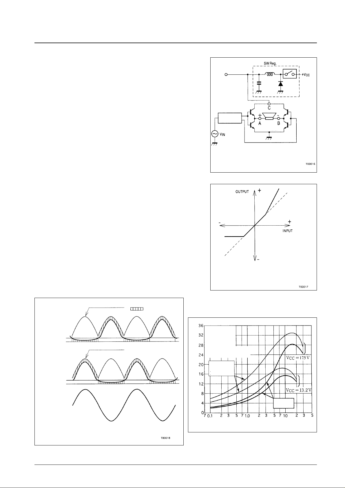
Technologies for Increased Efficiency Used in the LA4906
• Nonlinear amplifier
The LA4906 adopts a nonlinear amplifier, which has the nonlinear
characteristics shown in Figure 2, in the signal system. The LA4906
dispenses with the lower side switching regulator by using a low 2 V
as the midpoint voltage instead of the 1/2 VCC used in normal
amplifiers.
This nonlinear amplifier is basically formed from a differential
amplifier that has a symmetrical negative feedback circuit. Although
the BTL output stage positive and reverse phase output waveforms
have a half-wave waveform that, when referenced to ground, is
expanded and compressed as shown in Figure 3, the combined
output waveform at the load terminals is identical to that of earlier
products.
• Signal-following switching technique
The LA4906 uses a switching regulator for the power supply for the
amplifier output stage. The LA4906 significantly reduces power
dissipation by having the switching regulator output voltage follow
the signal. Also, the LA4906 restricts the number of switching
regulators required to just one circuit even though it implements a
BTL 2-channel amplifier by using the switching regulator in
combination with the nonlinear amplifier described below. (See
Figure 1.)
Figure 1 Overview Block Diagram
Figure 2 Nonlinear Amplifier
Input/Output Characteristics
Figure 3 Output Waveforms
Figure 4
RL = 4 Ω
f = 1 kHz
Rg = 600 Ω
With both channels
driven.
Calculated at Pd =
VCC × ICC – 2 P
O
Regulator
output
Amplifier
output
stage
Nonlinear
amplifier
Loss in the output
transistor
Regulator output (point C)
Regulator output (point C)
Positive phase
output (point A)
Center point
Ground
Reverse phase
output (point B)
Center point
Ground
Waveform between
the outputs
(Between A and B)
Power dissipation, Pd – W
Output power, PO– W
High-efficiency
LA4906
Earlier SANYO
products (class
B amplifiers)
 Loading...