

SANYO LA4905 Datasheet
Overview
The LA4905 is a BTL 2-channel power amplifier IC for
use in car audio systems. Increases in the number of
external components are held to a minimum by adopting
both a signal-following type switching scheme in the
amplifier’s output stage power supply, and a newlydeveloped nonlinear amplifier that has nonlinear
characteristics in the signal system. The power dissipation
(thermal loss) in the actual operating range has been
reduced to about 1/2 that of earlier class B amplifier ICs.
This contributes significantly to miniaturization of the heat
sink and to reduction of heating within the set.
Features
• Power dissipation reduced by 50% (When average
music power is measured, and when compared to earlier
Sanyo products.)
• The number of required signal follower circuits has been
reduced to a single circuit for two channels, allowing the
number of external components to be reduced.
• The output is a pure analog signal: no switching noise is
output to the output lines.
• Operates on an 8 to 18-V single-voltage power supply.
• Full complement of built-in protection circuits (shorting
to the power supply, shorting to ground, overvoltage,
and thermal protection)
• Built-in standby switch
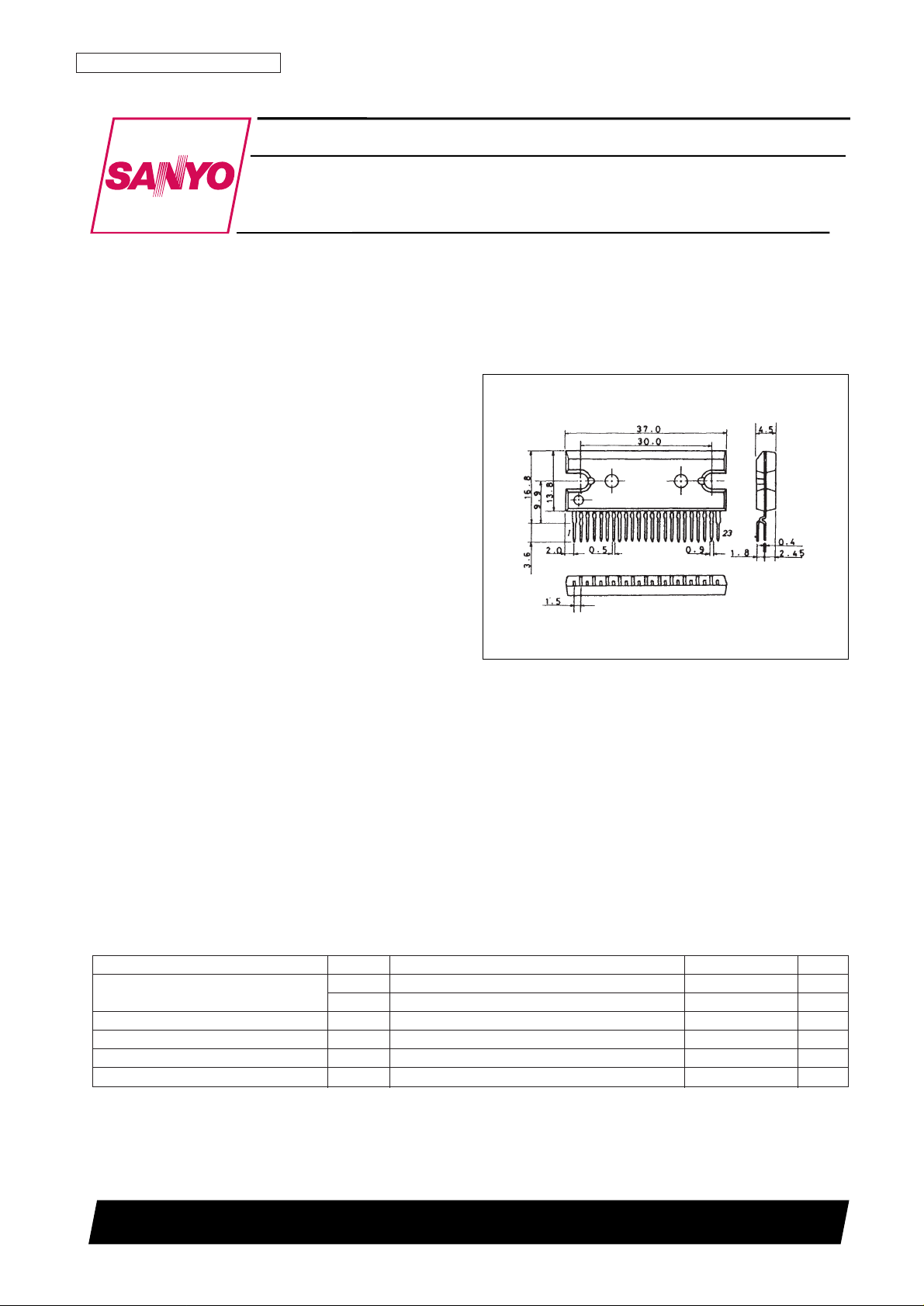
Package Dimensions
unit: mm
3160-SIP23HZ
Monolithic Linear IC
Ordering number : EN5504
83096HA (OT) No. 5504-1/10
SANYO: SIP23HZ
[LC4905]
SANYO Electric Co.,Ltd. Semiconductor Bussiness Headquarters
TOKYO OFFICE Tokyo Bldg., 1-10, 1 Chome, Ueno, Taito-ku, TOKYO, 110 JAPAN
17-W, 2-Channel BTL AF High-Efficiency
Power Amplifier for Car Stereo Systems
LA4905
Parameter Symbol Conditions Ratings Unit
Maximum supply voltage
V
CC
max1 No input, t = 1 minute 24 V
V
CC
max2 18 V
Maximum output current I
O
Peak (Per channel) 4.5 A
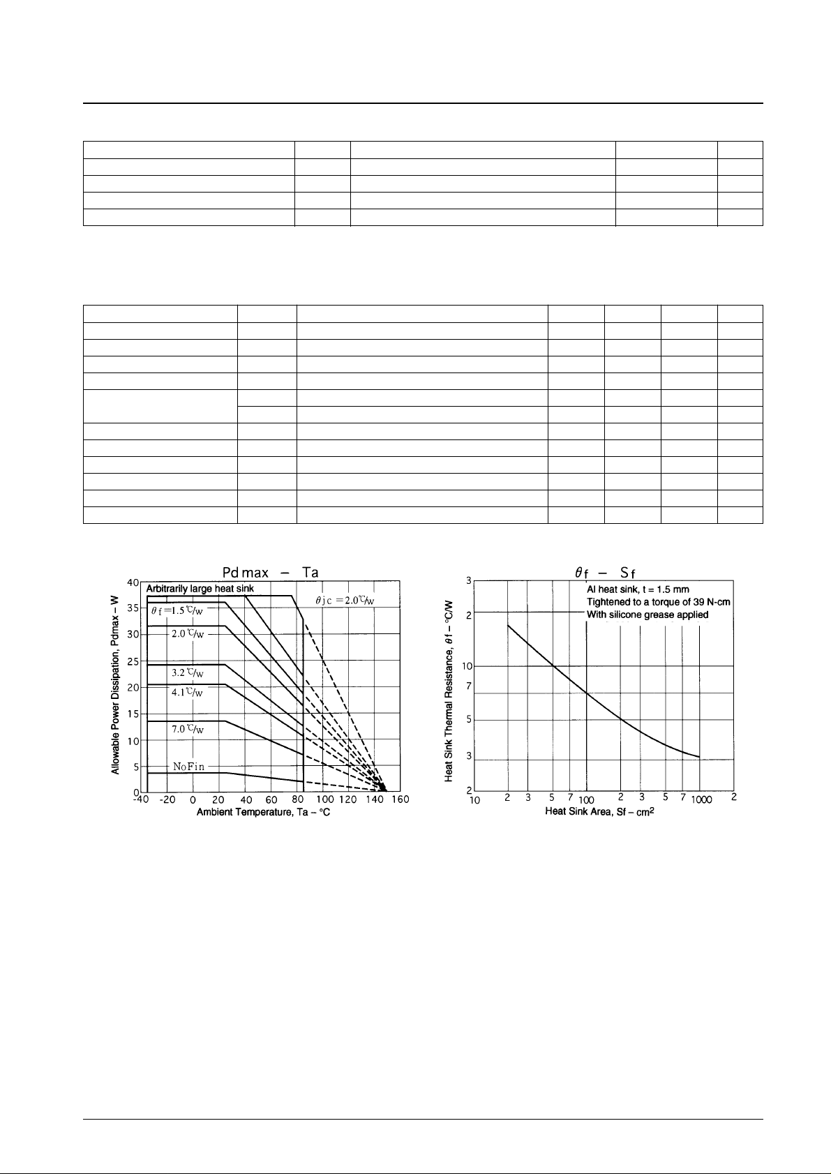
Allowable power dissipation Pd max With an arbitrarily large heat sink 37.5 W
Operating temperature Topr –35 to +85 °C
Storage temperature Tstg –40 to +150 °C
Specifications
Maximum Ratings at Ta = 25°C
Notes: 1. Set VCC and RL in the range where Pd max does not exceed 37.5 W.
2. The overvoltage protection circuit operates when VCC is 20 V or higher.
No. 5504-2/10
LA4905
Parameter Symbol Conditions Ratings Unit
Recommended supply voltage V
CC
13.2 V
Allowable operating supply voltage range V
CC
op 8 to 18 V
Recommended load resistance R
L
4 Ω
Recommended load resistance range R
L
op 2 to 4 Ω
Operating Conditions at Ta = 25°C
Operating Characteristics at Ta = 25°C, VCC= 13.2 V, RL= 4 Ω, f = 1 kHz, Rg = 600 Ω, in the recommended circuit
Notes:Set VCC and RL in the range where Pd max does not exceed 37.5 W.
Parameter Symbol Conditions min typ max Unit
Quiescent current Icco R
L
= ∞, VIN= 0 80 110 150 mA
Standby current Ist 0 10 µA
Voltage gain VG V
O
= 0 dBm 38 40 42 dB
Total harmonic distortion THD P
O
= 1W, LPF = 30 kHz 0.07 0.2 %
Output power 1
P
O
1 THD = 10%, RL= 4 Ω 14 17 W
P
O
2 THD = 10%, RL= 2 Ω 25 W
Output noise voltage V
NO
Rg = 0, BPF = 20 Hz to 20 kHz 0.15 0.3 mVrms
Ripple rejection ratio SVRR Rg = 0, V
CCR
= 0 dBm, BPF = 20 Hz to 20 kHz 60 70 dB
Channel separation CHsep Rg = 10 kΩ, V
O
= 0 dBm, BPF = 20 Hz to 20 kHz 45 55 dB
Input resistance Ri 21 30 39 kΩ
Output offset voltage VN offset Rg = 0 –300 +300 mV
Standby on voltage V
STH
AMP = on, applied through a 10 kΩ resistor 3 V
CC
V
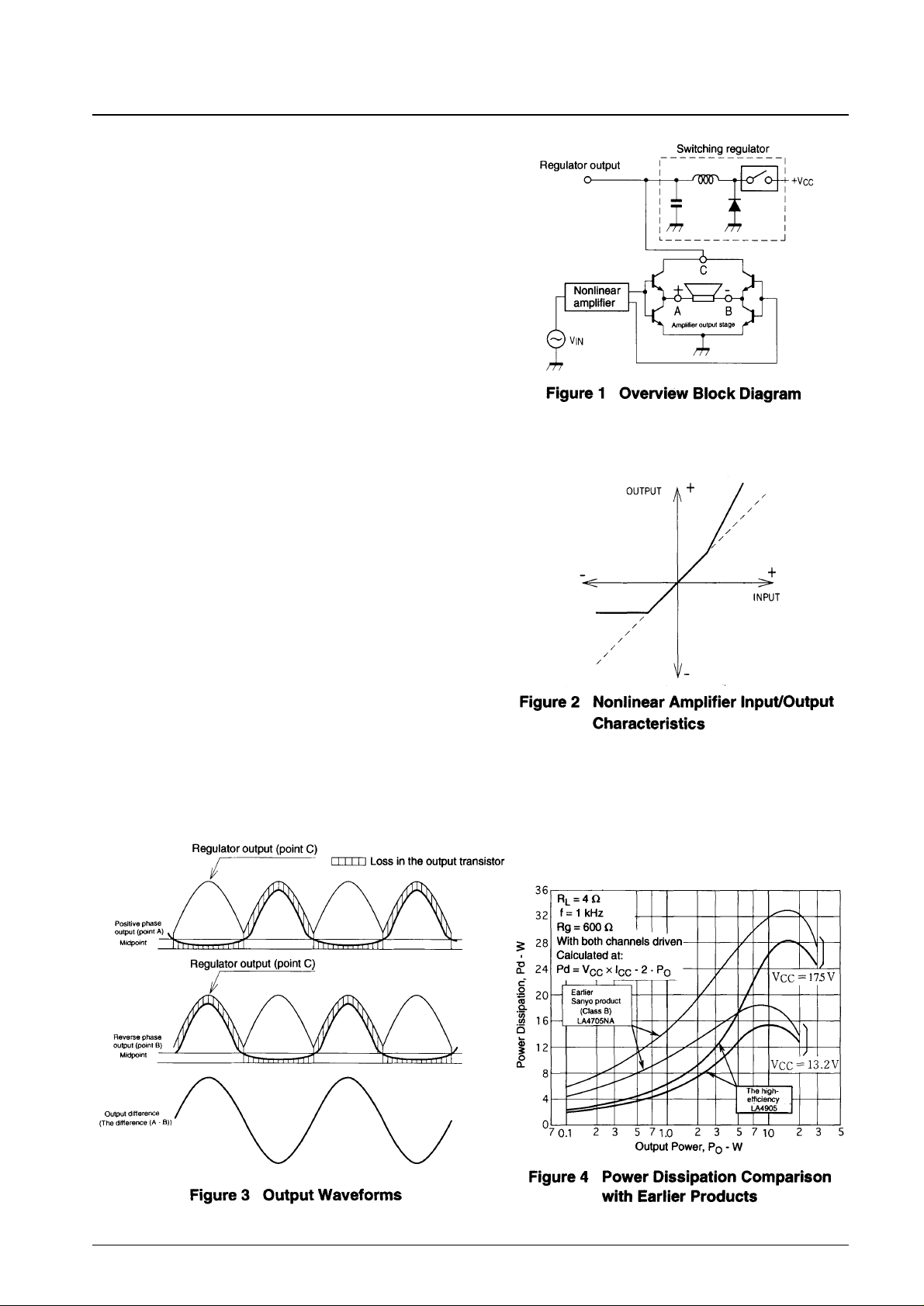
LA4905 High-Efficiency Technology
(1) Signal-following switching scheme
The LA4905 adopts a switching regulator scheme in
the power supply applied to the amplifier output stage.
The LA4905 power dissipation is reduced significantly
by having the output voltage of the switching regulator
follow the input signal. Furthermore, in combination
with the nonlinear amplifier scheme described below,
the LA4905 design reduces the number of switching
regulators to merely one circuit even though it is a
BTL 2-channel amplifier. (See Figure 1.)
(2) Nonlinear amplifier
The LA4905 adopts a nonlinear amplifier that has the
nonlinear characteristics shown in Figure 2 in the
amplifier signal system. This scheme does not use the
center point voltage of 1/2 VCC used in normal
amplifiers, but instead uses a voltage about 2 V lower.
This allows the design to dispense with the lower side
switching regulator.
This nonlinear amplifier has a structure based on a
differential amplifier that has symmetric negative
feedback circuits. Although the BTL output stage
positive and negative phase output waveform is a halfwave waveform that is expanded and compressed as
shown in Figure 3, the combined output waveform at
the negative load terminal is identical to that output by
earlier products.
No. 5504-3/10
LA4905
 Loading...