

SANYO LA4820M Datasheet
Ordering number: EN5205A
Monolithic Linear IC
LA4820M
Monaural Speaker/Stereo Headphone
Power Amplifier
Overview
The LA4820M compound power IC is designed for portable
information processing equipment, such as electronic book
players and personal notebook computers, and provides on chip
headphone stereo amplifier and monaural speaker amplifier
functions required of such devices. This system IC also
provides on chip a power-saving headphone jack plug-in/out
detection function, which automatically switches the amplifiers,
and an optimum volume level controller.
Features
c Power-saving headphone jack plug-in/out detection function
on chip that electronically switches between the stereo
headphone amplifier and the monaural BTL amplifier
according to jack plug-in/out.
c The monaural amplifier has, as output control functions, a
built-in output limiter that permits adjustment in accordance
with the speaker impedance and a non-clipping circuit that
outputs a sine wave suited to the output D range, while the
headphone amplifier has a built-in user-friendly PVSS (Peak
Volume Select System).
c On-chip ripple filter with a high ripple rejection ratio in
order to reduce power line noise.
c Less external components needed thanks to system and
circuit technology, and low-capacitance design (22 µF or
less) allowing support for chip components.
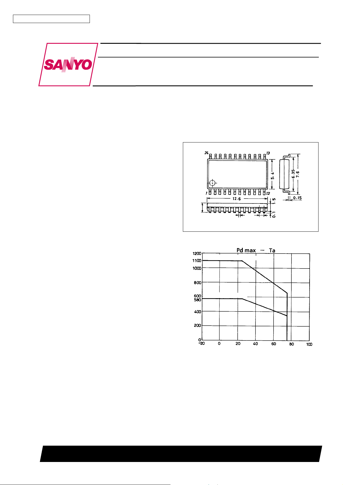
Package Dimensions
unit : mm
3112-MFP24S
[LA4820M]
SANYO : MFP24S
Sanyo recommended board
Independent IC
Functions
c Monaural BTL power amplifier
c Headphone OCL power amplifier (16 Ω) × 2
c Output control functions:
Headphone power PVSS
Monaural power Non-clipping circuit and output
limiter
c Headphone jack plug-in/out detection function
(monaural amplifier/headphone amplifier switching)
c Ripple filter
c Power mute switch
c Common amplifier on/off switching
Allowable power dissipation, Pd max − mW
Ambient temperature, Ta −°C
SANYO Electric Co.,Ltd. Semiconductor Bussiness Headquarters
TOKYO OFFICE Tokyo Bldg., 1-10, 1 Chome, Ueno, Taito-ku, TOKYO, 110 JAPAN
22896HA(II) No.5205-1/20
LA4820M
Specifications
Maximum Ratings atTa=25°C
Parameter Symbol Conditions Ratings Unit
Maximum supply voltage V
Allowable power dissipation Pd max 580 mW
Operating temperature Topr –20 to +75
Storage temperature Tstg –40 to +150
Operating Conditions atTa=25°C
Parameter Symbol Conditions Ratings Unit
Recommended supply voltage V
Operating voltage range V
Operating Characteristics atTa=25°C, VCC1 = 6.0 V, fi = 1 kHz, 0.775 V = 0 dBm,
Parameter Symbol Conditions min typ max Unit
[Total]
Quiescent current I
Input resistance Ri 10 13 16 kΩ
[Monaural Amplifier]
Output power P
Voltage gain (closed) VG1 V
Total harmonic distortion THD1 P
Output noise voltage V
Ripple rejection ratio Rr1 Rg = 0 Ω, Vr = −10 dBm, fr = 100 Hz 60 77 dB
DC offset voltage V
[Non-clipping + Monaural Amplifier]
Output power P
Total harmonic distortion THD2 Vi = 0 dBM 1.2 2.0 %
[Output Limiter + Monaural Amplifier]
Output power P
Total harmonic distortion THD3 Vi = 0 dBm, output limiter input resistance 220 Ω 0.5 1.2 %
[Headphone Amplifier]
Output power P
Voltage gain (closed) VG2 V
Total harmonic distortion THD4 P
Interchannel crosstalk CT VO = –5 dBm, Rg = 0 Ω 30 39 dB
Output noise voltage V
Ripple rejection ratio Rr2 Rg = 0 Ω, Vr = −10 dBm, fr = 100 Hz 70 92 dB
DC offset voltage V
[PVSS + Headphone Amplifier]
PVSS voltage V
PVSS distortion factor THD5 Vi = –30 dBm, PVSS2 0.25 1.6 %
PVSS start input V
PVSS width W
[Ripple Filter]
Output voltage V
Ripple rejection ratio Rr3
1,2 max 8.0 V
CC
With Sanyo evaluation board (84.2 × 92.6 mm2)
1 6.0 V
CC
1 op 2.5 to 7.2 V
CC
V
2 op 2.0 to 7.2 V
CC
=16Ω: monaural amplifier, RL=16Ω: headphone amplifier
R
L
1 Rg=0kΩ, monaural amplifier 7.0 11.5 21.0 mA
CCO
I
2 Rg=0kΩ, headphone amplifier 5.5 9.0 14.0 mA
CCO
I
3 Headphone common amplifier off 4.0 6.3 10.0 mA
CCO
1 THD = 10%, pin 12 connected to GND 500 760 mW
O
1 Rg=0Ω, BPF = 20 to 20 kHz 170 300 µV
NO
1 Between pin 19 and pin 21 –80 0 +80 mV
OFF
2 Vi = 0 dBm 300 450 mW
O
3 Vi = 0 dBm, output limiter input resistance 220 Ω 120 200 300 mW
O
4 THD = 10% 30 120 mW
O
2 Rg=0Ω, BPF = 20 to 20 kHz 16 35 µV
NO
2 Between pin 15 and pin 16, and pin 16 and pin 17 –40 0 +40 mV
OFF
O
OPi
PVSS
RF
= 0 dBm 36.0 39.0 42.0 dB
O
= 100 mW 0.1 1.0 %
O
= –10 dBm 15.3 18.3 21.3 dB
O
= 1 mW 0.1 0.5 %
O
Vi = –30 dBm, PVSS2 –39 –36 –33 dBm
PVSS2 –59 –55 –51 dBm
Input width from the starting point to the point
where the output is +4 dB, PVSS ON
IRF= 300 mA, 2SB1295 hFE6 used 5.30 5.49 5.70 V
Vr = –10 dBm, fr = 100 Hz, I
2SB1295 h
FE
6 used
= 300 mA,
RF
28 35 dB
30 34 dB
1.1 W
C
°
C
°
No.5205-2/20
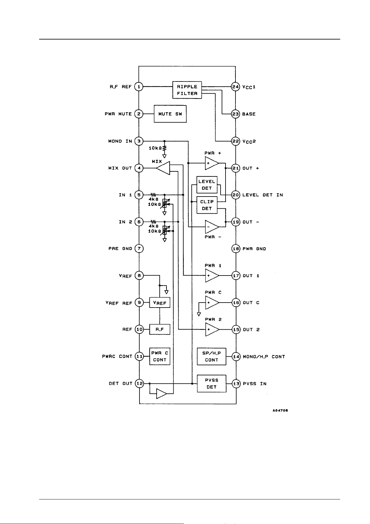
Block Diagram
LA4820M
No.5205-3/20
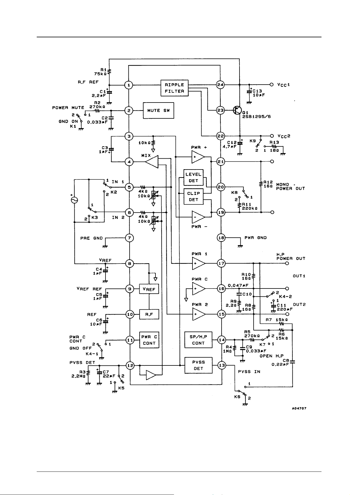
Test Circuit Diagram
LA4820M
No.5205-4/20
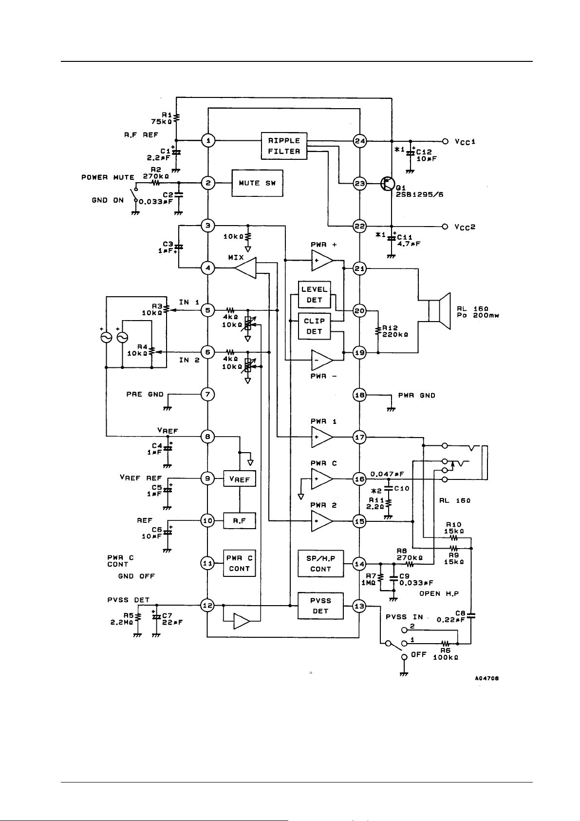
Sample Application Circuit 1
LA4820M
*1 A Tantalum capacitor is recommended.
*2 A polyester film or ceramic capacitor (of which capacitance specified must be independent of temperature changes) is
recommended.
No.5205-5/20
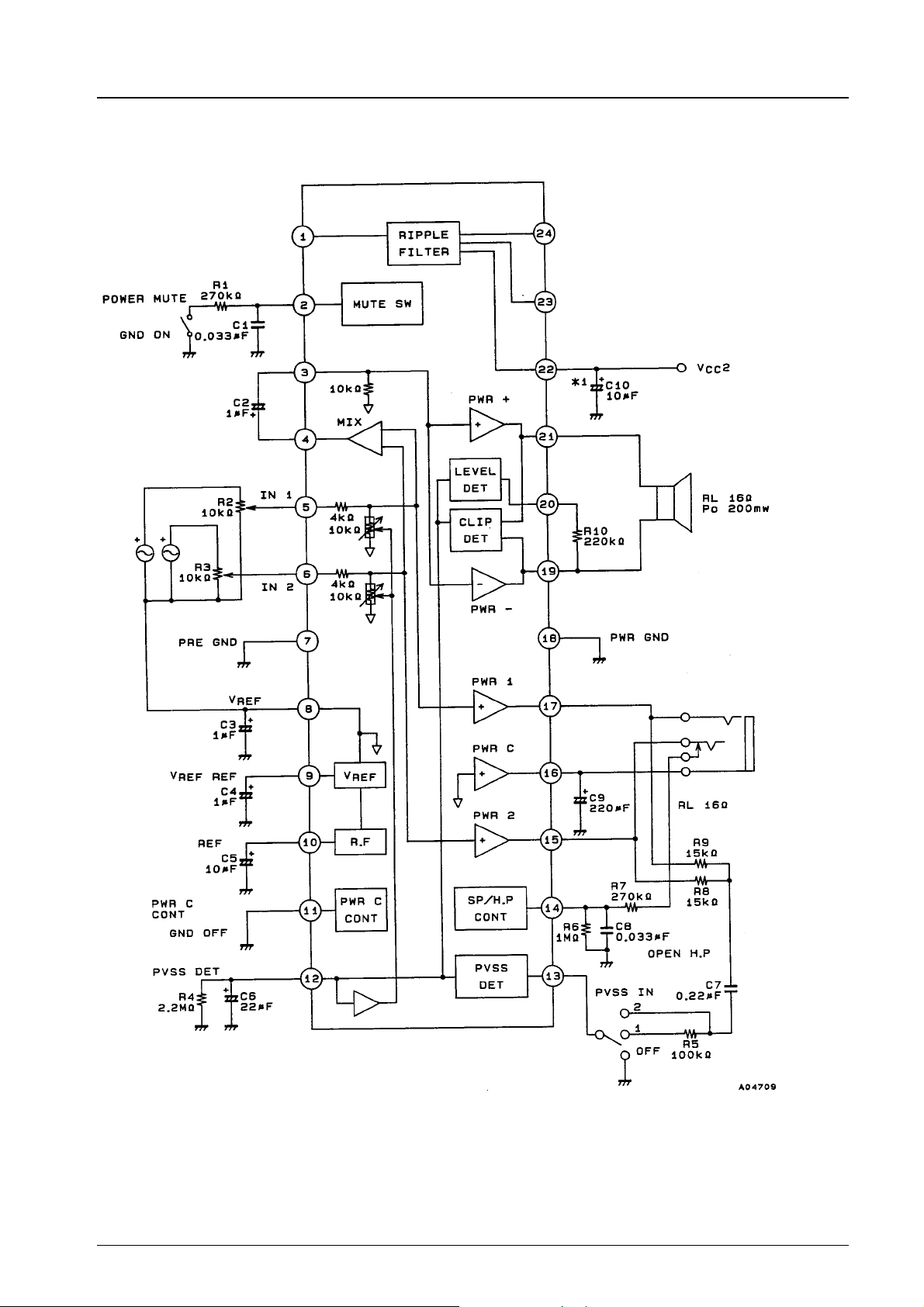
Sample Application Circuit 2
(When neither ripple filter nor common amplifier is used.)
LA4820M
*1 A Tantalum capacitor is recommended.
No.5205-6/20
 Loading...