

Sanyo LA4805V Specifications

Ordering number : EN4469A
O3098HA (OT)/40794TH B8-0242 No. 4469-1/17
LA4805V
SANYO Electric Co.,Ltd. Semiconductor Bussiness Headquarters
TOKYO OFFICE Tokyo Bldg., 1-10, 1 Chome, Ueno, Taito-ku, TOKYO, 110-8534 JAPAN
3 V Stereo Headphone Power Amplifier
Monolithic Linear IC
Any and all SANYO products described or contained herein do not have specifications that can handle
applications that require extremely high levels of reliability, such as life-support systems, aircraft’s
control systems, or other applications whose failure can be reasonably expected to result in serious
physical and/or material damage. Consult with your SANYO representative nearest you before using
any SANYO products described or contained herein in such applications.
SANYO assumes no responsibility for equipment failures that result from using products at values that
exceed, even momentarily, rated values (such as maximum ratings, operating condition ranges, or other
parameters) listed in products specifications of any and all SANYO products described or contained
herein.
Overview
The LA4805V is a power IC developed for use in stereo
headphones. It includes low frequency enhancement, beep
function and output control circuits on-chip. Furthermore,
the LA4805V realizes a high S/N ratio, a high ripple
exclusion ratio, and low current drain.
Functions
• Stereo headphone power amplifier
• Low frequency enhancement (L.BOOST)
• Beep amplifier
• Output suppression circuit (PVSS)
• Power switch
• Muting switch
Features
• Low current drain (8.3 mA typical)
• High S/N ratio (90 dB typical, 13 µV)
• High ripple exclusion ratio (75 dB typical)
• No output electrolytic capacitors required
• Ultra-miniature package (SSOP-30)
Package Dimensions
unit: mm
3191-SSOP30
Specifications
Maximum Ratings at Ta = 25°C
Operating Conditions at Ta = 25°C
Parameter Symbol Conditions Ratings Unit
Maximum supply voltage V
CC
max 4.5 V
Allowable power dissipation Pd max 500 mW
Operating temperature Topr –15 to +50 °C
Storage temperature Tstg –40 to +150 °C
Parameter Symbol Conditions Ratings Unit
Recommended supply voltage V
CC
3.0 V
Recommended load resistance R
L
16 to 32 Ω
Operating supply voltage range V
CC
op 1.8 to 3.6 V
SANYO: SSOP30
[LA4805V]

Operating Characteristics
at Ta = 25°C, V
CC
= 3.0 V, f = 1 kHz, 0.775 V = 0 dBm, RL= 10 kΩ (L.B), RL= 16 Ω (PWR)
Note: * Boost levels relative to 1 kHz
No. 4469-2/17
LA4805V
Parameter Symbol Conditions
Ratings
Unit
min typ max
[L.BOOST +PVSS + PWR]
I
CCO
1 IC off 0.05 1.0 µA
Quiescent current
I
CCO
2 Muting on 1.0 2.7 5.0 mA
I
CCO
3 Rg = 0, L.BST/PVSS off 4.0 8.3 12.0 mA
I
CCO
4 Rg = 0, L.BST/PVSS on 4.5 8.6 12.5 mA
[PWR AMP]
Output power P
O
THD = 10% 15 25 mW
Voltage gain VG1 V
O
= –10 dBm 15.7 17.7 19.7 dB
Channel balance V
BL
VO= –10 dBm –1 0 1 dB
Total harmonic distortion THD1 V
O
= 0.35 V 0.1 0.3 %
Output noise voltage V
NO
1 Rg= 0, DIN AUDIO 13 25 µV
Crosstalk CT1 V
O
= –10 dBm, TUN = 1 kHz, Rg = 0 35 45 dB
Ripple exclusion ratio SVRR1
V
CC
= 1.8 V, f = 100 Hz, VR= –20 dBm,
60 75 dB
TUN = 100 Hz
Muting attenuation ATT
M
THD = 1%, Rg = 0 kΩ 80 90 dB
Beep output V
O BEEPVIN
= –16 dBm (sine wave) 1.0 3.0 mV
Output current offset V
DC OFFVIN
= 0 V, Rg = 0 –20 0 20 mV
Input resistance Ri 7 10 13 kΩ
[L.BOOST]
Voltage gain VG2 V
IN
= –30 dBm, boost on/off –3.2 –5.2 –7.2 dB
Boost*
L.BTS1 V
IN
= –30 dBm, f = 100 Hz, boost on 13 15 17 dB
L.BTS2 V
IN
= –30 dBm, f = 10 kHz, boost on 3 5 7 dB
Maximum output voltage V
O
max THD = 1%, boost on 0.2 0.4 0.6 V
Total harmonic distortion THD2 V
O
= 0.1 V, boost on 0.085 0.25 %
Crosstalk CT2 V
O
= –20 dBm, Rg = 0, boost on 25 30 dB
Output noise voltage V
NO
2 Rg = 0, boost off 3 10 µV
Ripple exclusion ratio SVRR2
Rg = 0, f = 100 Hz, Vg = –20 dBm,
50 60 dB
boost on
[L.BOOST + PWR]
Voltage gain VG3 V
IN
= –30 dBm, f = 1 kHz, boost on/off 8 10 12 dB
Output voltage V
O
1 VIN= –30 dBm, f = 100 Hz, boost on 0.13 0.23 0.33 V
Total harmonic distortion THD3 V
IN
= –30 dBm, f = 100 Hz, boost on 0.14 0.5 %
Crosstalk CT3 V
O
= –20 dBm, RV= 0 Ω, boost on 25 32.5 dB
[L.BOOST + PVSS + PWR]: When V
O
1 is maximum
PVSS voltage V
O PVSS
2 VIN= –30 dBm, PVSS2 –32.5 –37.5 –42.5 dBm
PVSS width V
O PVSS
W
The input amplitude when the output is
25 30 35 dB
+3 dB over the starting point
PVSS distortion THD
PVSSVIN
= –40 dBm, PVSS2 0.55 2.0 %
PVSS starting input V
IN PVSS
PVSS2 –41 –46 –51 dBm
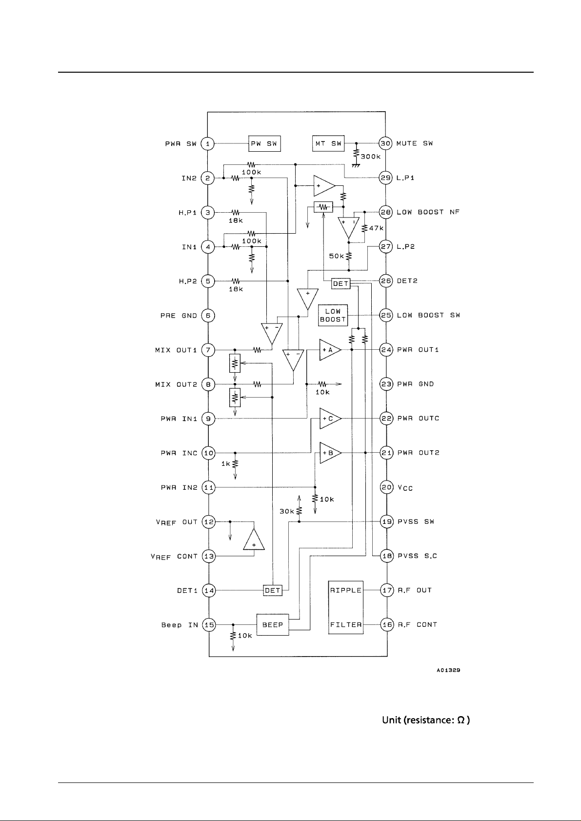
Pin Assignment and Block Diagram
No. 4469-3/17
LA4805V
Test Circuit
No. 4469-4/17
LA4805V
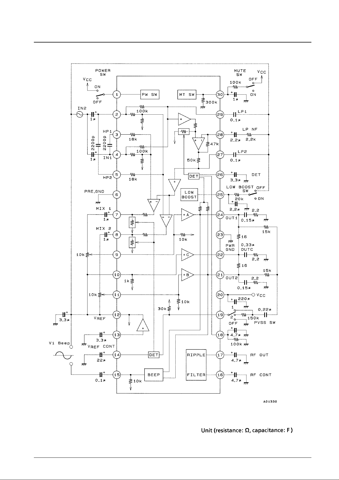
Sample Application Circuit
No. 4469-5/17
LA4805V
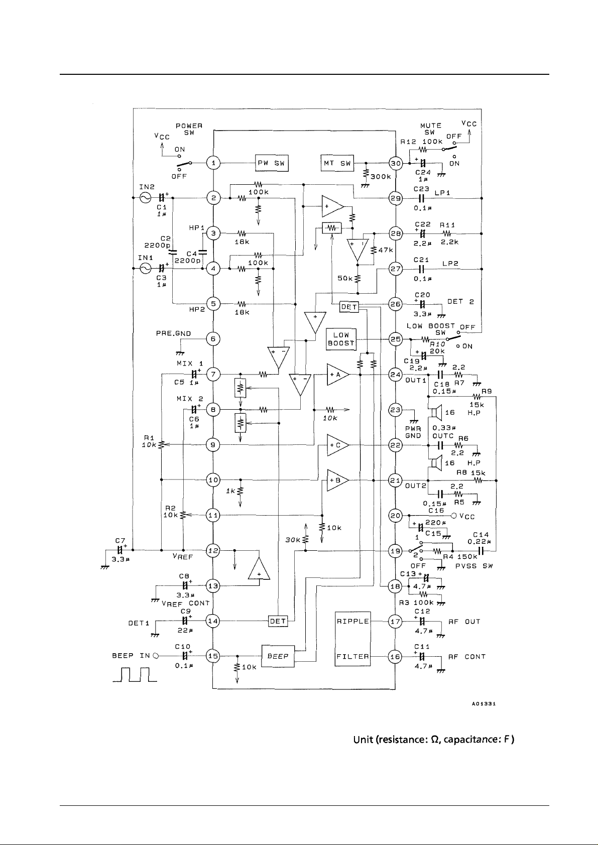
Pin Functions and Equivalent Circuits (VCC= 3.0 V)
No. 4469-6/17
LA4805V
Pin No. Symbol VDC(V) Equivalent circuit Pin function
1 PWR SW 0 to 0.7
2 IN 2 1.1
4 IN 1 1.1
3 H.P 1 1.1
5 H.P 2 1.1
7 MIX OUT 1 1.1
8 MIX OUT 2 1.1
9 PWR IN 1 1.1
11 PWR IN 2 1.1
10 PWR IN C 1.1
6 PRE GND
• Applying V
CC
to pin 1 turns the IC power on.
• Low boost input pin
• High-pass input pin
• Low boost and buffer output pin
• Power input pin
• The input resistance is 10 kΩ.
• Power amp common input pin
• Connect to Vref in normal operation
Continued on next page.
Unit (resistance: Ω)
 Loading...