

SANYO LA4802T Datasheet
Ordering number : ENN6657
72502RM (OT) No. 6657-1/10
Overview
The LA4802T is a headphone stereo power amplifier for
portable CD and MD players. It features a high signal-tonoise ratio, a high ripple rejection ratio, low distortion,
and low current drain.
Functions
• Headphone stereo power amplifier
• Power switch
• Muting switch
• Beep tone function control input pin (The beep tone
function can be used regardless of whether the mute
function is on or off.)
Features
• High signal-to-noise ratio (100 dB typical at 7.5 µV)
• High ripple rejection ratio (70 dB typical)
• Low current drain (950 µA typical)
• On-chip bass compensation circuit
(Compensates for bass frequency attenuation due to the
output capacitors and achieves flat frequency
characteristics.)
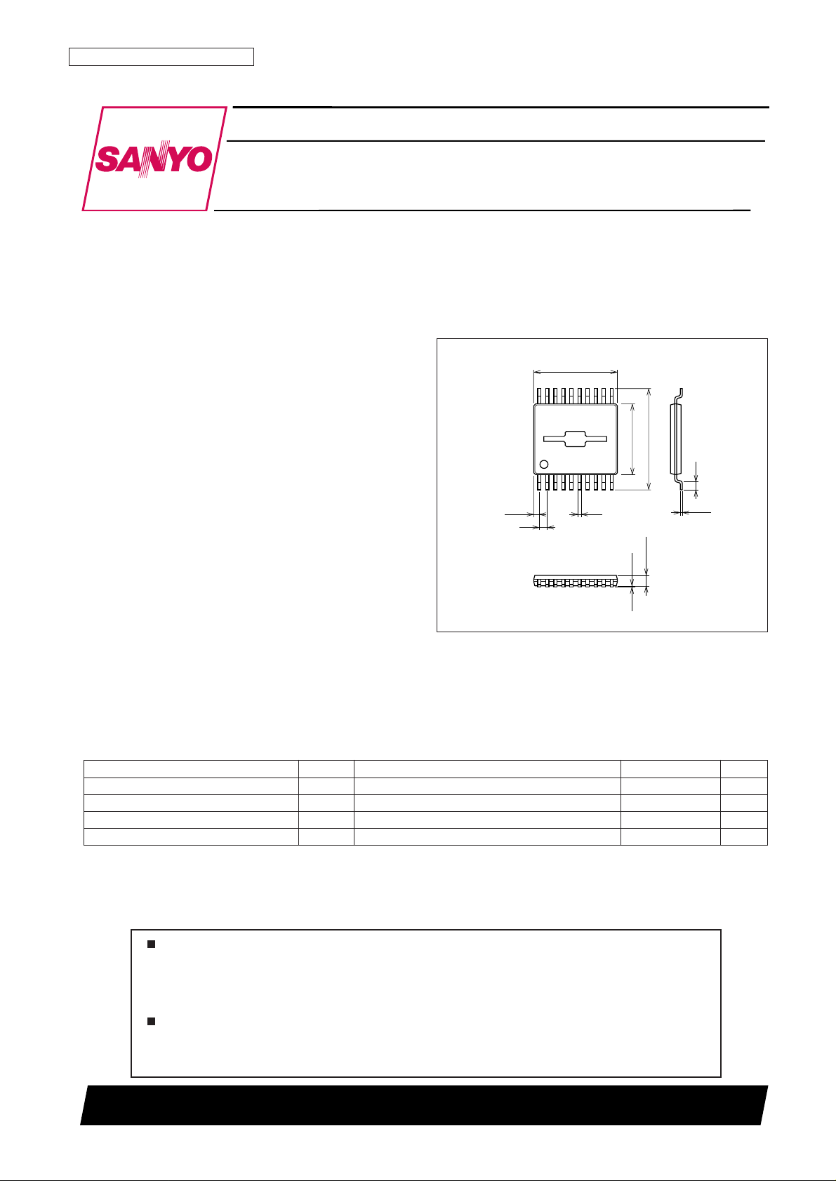
• Ultraminiature package (MSOP-20)
Package Dimensions
unit: mm
3262-MSOP20
6.3
5.2
0.5
4.4
(0.35)
(0.65)
0.5
0.125
1
10
20 11
0.2
0.08
0.85max
SANYO: MSOP20
[LA4802T]
LA4802T
SANYO Electric Co.,Ltd. Semiconductor Company
TOKYO OFFICE Tokyo Bldg., 1-10, 1 Chome, Ueno, Taito-ku, TOKYO, 110-8534 JAPAN
Headphone Stereo Power Amplifier
Monolithic Linear IC
Any and all SANYO products described or contained herein do not have specifications that can handle
applications that require extremely high levels of reliability, such as life-support systems, aircraft’s
control systems, or other applications whose failure can be reasonably expected to result in serious
physical and/or material damage. Consult with your SANYO representative nearest you before using
any SANYO products described or contained herein in such applications.
SANYO assumes no responsibility for equipment failures that result from using products at values that
exceed, even momentarily, rated values (such as maximum ratings, operating condition ranges, or other
parameters) listed in products specifications of any and all SANYO products described or contained
herein.
Parameter Symbol Conditions Ratings Unit
Maximum supply voltage V
CC
max 4.5 V
Allowable power dissipation Pd max When mounted, Ta = 80°C 375 mW
Operating temperature Topr –20 to +80 °C
Storage temperature Tstg –40 to +150 °C
Specifications
Maximum Ratings at Ta = 25°C
No. 6657-2/10
LA4802T
Parameter Symbol Conditions Ratings Unit
Recommended supply voltage V
CC
2.4 V
Operating supply voltage range V
CC
op 1.8 to 3.6 V
Recommended load resistance R
L
16 to 32 Ω
Operating Conditions at Ta = 25°C
Item Symbol Conditions
Ratings
Unit
min typ max
Quiescent current I
CCO
1
Current when ST is off (with L.B. on and muting off)
0.05 1 µA
I
CCO
2
Current when muting is on (with ST on and L.B. on)
530 900 µA
I
CCO
3
Current when ST is on (with L.B. on and muting off)
950 1500 µA
Operating current drain I
CC
1 PO= 0.1 mW (With 2 channels driven) 3.2 3.7 mA
Voltage gain VG V
O
= –10 dBm 6.8 7.8 8.8 dB
Channel balance ∆VG V
O
= –10 dBm –1 0 +1 dB
Output power P
O
THD = 10% 25 38 mW
Total harmonic distortion THD V
O
= –8 dBm, 20 kHz LPF 0.03 0.1 %
Output noise voltage V
NO
Rg = 10 kΩ, IHF A –100 –90 dBm
Crosstalk CT T
UN
1kHz, VO= –10 dBm 70 80 dB
Ripple rejection ratio SVRR fr = 100 kHz, Vr = –20 dBm, T
UN
100Hz 60 70 dB
Peak output voltage V
O
BEEP VIN= 2.4 Vp-p, f = 1 kHz, MUTE OFF 1.0 2.7 mV
Muting attenuation V
OFF
THD = 1%, TUN1kHz –100 –120 dB
Power on voltage sensitivity V
1 ON
Power on threshold voltage 1.6 V
Power off voltage sensitivity V
1 OFF
Power off threshold voltage 0.5 V
Mute on voltage sensitivity V
20 ON
Muting on threshold voltage 1.4 V
Mute off voltage sensitivity V
20 OFF
Muting off threshold voltage 0.5 V
Boost on voltage sensitivity V
4 ON
Boost on threshold voltage 0.5 V
Boost off voltage sensitivity V
4 OFF
Boost off threshold voltage 1.4 V
Ta = 25°C, V
CC
= 2.7 V, fIN= 1 kHz, RL= 47 kΩ (Characteristics when used as a line output), L.B OFF
Operating current drain I
CC
2 VO= 0 dBm (With 2 channels driven) 1.5 2.0 mA
Total harmonic distortion THD2 V
O
= 0 dBm, 20 kHz LPF 0.005 0.05 %
Output noise voltage V
NO
2 Rg = 10 kΩ, IHF A –100 –90 dBm
Crosstalk CT2 T
UN
1kHz, VO= –10 dBm 80 90 dB
Ripple rejection ratio SVRR2 fr = 100 kHz, Vr = –20 dBm, T
UN
100Hz 65 78 dB
Electrical Characteristics at Ta = 25°C, VCC= 2.4 V, fIN= 1 kHz, RL= 16 Ω
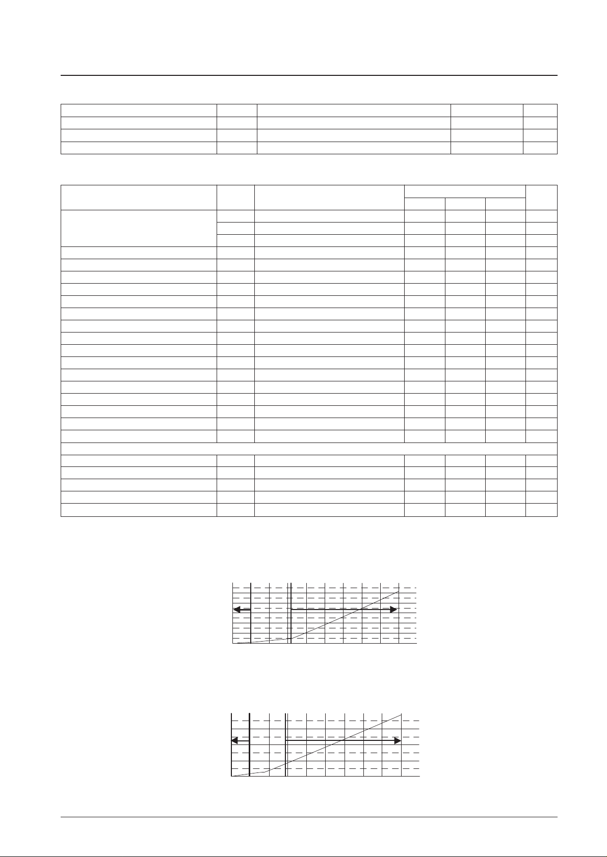
Switch Threshold Voltages and Pin Influx Currents
• Standby switch (pin 1)
H : IC ON
L : IC OFF
Pin influx current (µA)
0
20
40
60
80
100
120
0 1 2 3 4 5
V
1
(V)
H
L
• Mute switch (pin 20), boost switch (pin 4)
Pin influx current (µA)
0
20
40
0
30
0 1 2 3 4 5
V
20,V4
(V)
H
L
H : MUTE ON, L. B OFF
L : MUTE OFF, L. B ON
No. 6657-3/10
LA4802T
Notes on the Beep Tone Output Function
• This function provides a beep tone output under control of the system microcontroller.
• The beep tone can be provided regardless of the on/off state of the muting function.
• The recommended beep input signal level is a square wave with VIN= 2.4 Vp-p. When the muting function is off, the
beep tone output, VOBEEP, will be 2.7 V rms, and when muting is on, the output will be 1.3 Vrms.
Notes on the Muting Time
• The muting on time and the muting off time can be modified by changing the value of the external capacitor C4
connected to pin 6. The recommended value for C4 is 1 µF. With lower values, impulse noise levels will increase.
• The on/off times will change as shown below when the value of C4 is varied.
C4 On time Off time
0.1 µF 0.2 ms 9 ms
0.47 µF 1 ms 40 ms
1 µF 2 ms 80 ms
• We recommend operating the mute switch at the same time as the power on/off switch (pin 1) to minimize impulse
noise at power on and off.
V
CC
MUTE S. W
PWR S. W
A13553
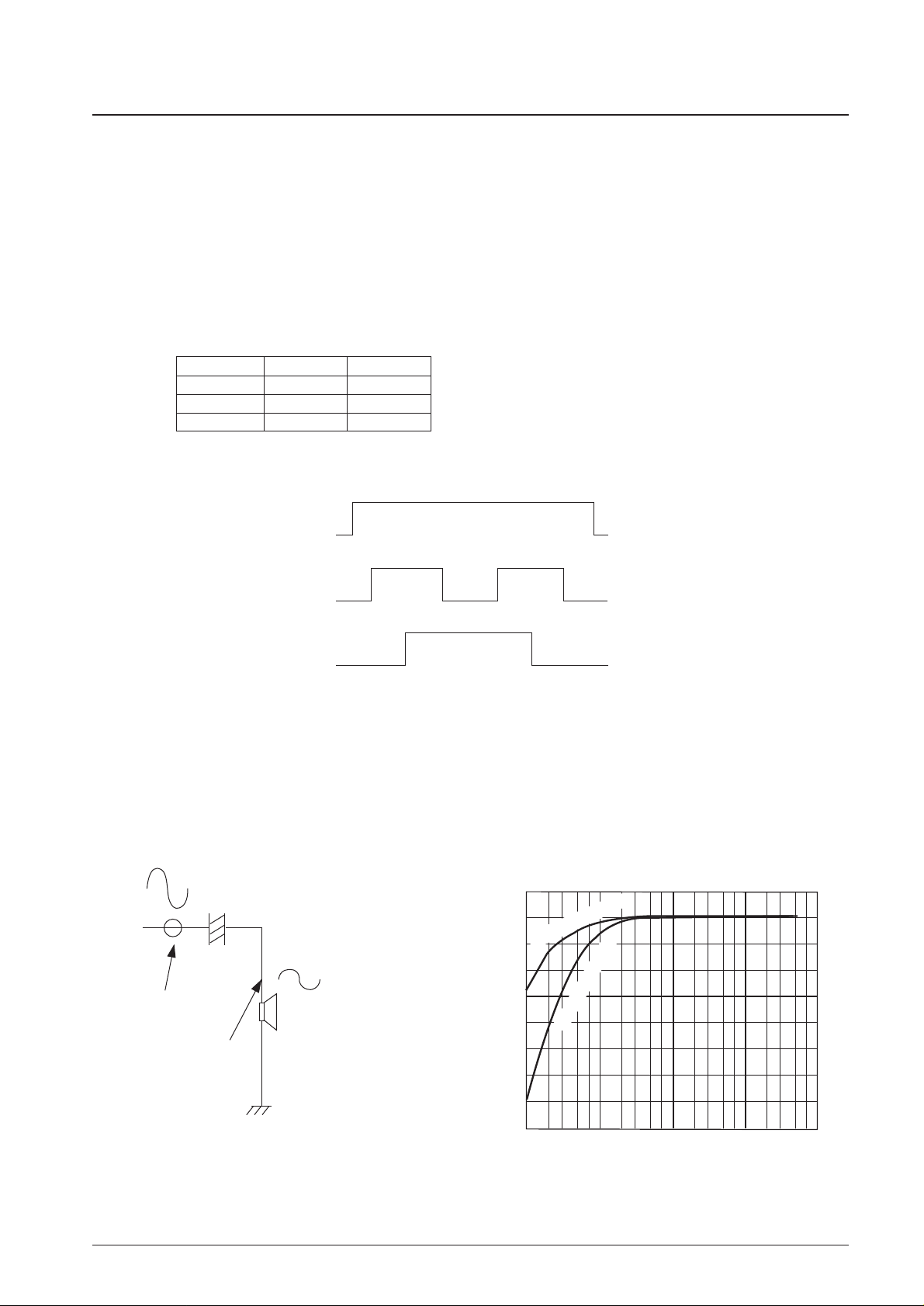
Notes on the Bass Compensation Circuit
• When the headphone load is connected to the output, the low frequencies will be attenuated due to the output
capacitors. This circuit compensates for that attenuation and creates frequency response characteristics that are close
to flat.
• This function can be turned on or off from pin 4. When used as a line output, the load will be less than 16 Ω, and the
bass frequency characteristics will be somewhat increased. Therefore we recommend leaving the bass compensation
circuit off in this case.
A13554
+
Output pin
Load terminal
–14
–12
–10
–8
–6
–4
–2
0
2
–16
10 100 1000 1k 10k
VG — f
Frequency, f — Hz
No bass compensation
Bass compensation applied
Voltage gain, VG — dB
 Loading...