

SANYO LA4801V Datasheet
Ordering number : ENN6146
72502RM (OT) No. 6146-1/10
Overview
The LA4801V is a headphone stereo power amplifier for
portable CD and MD players. It features a high signal-tonoise ratio, a high ripple rejection ratio, low distortion,
and low current drain.
Functions
• Headphone stereo power amplifier
• Power switch
• Muting switch
• Center amplifier switch
Features
• High signal-to-noise ratio (96 dB typical at 7 µV)
• High ripple rejection ratio (76 dB typical)
• Low current drain (4.8 mA typical)
• Low power consumption achieved through the use of a
dual power supply system.
• No electrolytic capacitors required for the outputs.
• Ultraminiature package (SSOP-16)
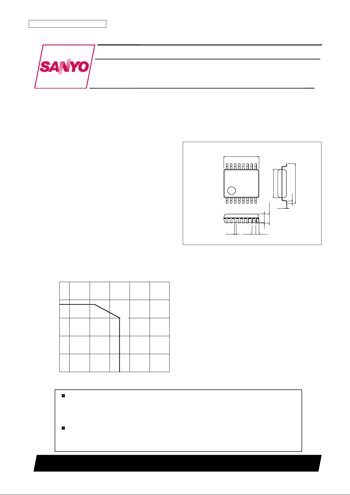
Package Dimensions
unit: mm
3178A-SSOP16
18
916
6.4
0.5
4.4
5.2
0.1
1.5max
0.65
0.22
(0.33)
0.15
(1.3)
SANYO: SSOP16 (225 mil)
[LA4801V]
LA4801V
SANYO Electric Co.,Ltd. Semiconductor Company
TOKYO OFFICE Tokyo Bldg., 1-10, 1 Chome, Ueno, Taito-ku, TOKYO, 110-8534 JAPAN
Headphone Stereo Power Amplifier
Monolithic Linear IC
Any and all SANYO products described or contained herein do not have specifications that can handle
applications that require extremely high levels of reliability, such as life-support systems, aircraft’s
control systems, or other applications whose failure can be reasonably expected to result in serious
physical and/or material damage. Consult with your SANYO representative nearest you before using
any SANYO products described or contained herein in such applications.
SANYO assumes no responsibility for equipment failures that result from using products at values that
exceed, even momentarily, rated values (such as maximum ratings, operating condition ranges, or other
parameters) listed in products specifications of any and all SANYO products described or contained
herein.
100
0
200
300
400
500
–10 0 20 40 60 80 100
Pd max — Ta
300
375
Ambient temperature, Ta — °C
Allowable power dissipation, Pdmax — mW
No. 6146-2/10
LA4801V
Parameter Symbol Conditions Ratings Unit
Maximum supply voltage V
CC
max 4.5 V
Allowable power dissipation Pd max 375 mW
Operating temperature Topr –15 to +50 °C
Storage temperature Tstg –40 to +150 °C
Specifications
Maximum Ratings at Ta = 25°C
Parameter Symbol Conditions Ratings Unit
Recommended supply voltage
V
CC
1 1.5 V
V
CC
2 2.5 V
Operating supply voltage range
V
CC
1 op 0.9 to 4.5 V
V
CC
2 op * 1.5 to 3.5 V
Recommended load resistance R
L
16 to 32 Ω
Operating Conditions at Ta = 25°C
Note: * However, when VCC2 is under 2.5 V, with a 1.5 V minimum, VCC1 must be less than or equal to VCC2.
Item Symbol Conditions
Ratings
Unit
min typ max
I
CCO
1 IC off: with pin 1 open. 0.05 1.0 µA
Quiescent current
I
CCO
2 Mute on 1.3 3.0 mA
I
CCO
3 Center amplifier off: with pin 3 at Vref 3.3 8.0 mA
I
CCO
4 No input 4.8 9.0 mA
Voltage gain VG V
O
= –10 dBm 10.3 11.8 13.3 dB
Channel balance ∆VG V
O
= –10 dBm –1 0 1 dB
Output power P
O
THD = 10% 6 13 mW
Total harmonic distortion THD P
O
= 0.5 mW 0.2 1.0 %
Output noise voltage V
NO
Rg = 1 kΩ, DIN AUDIO 7.8 15 µV
Crosstalk CT T
UN
1kHz, VO= –10 dBm 35 45 dB
Ripple rejection ratio SVRR
VCC= 1.0 V, fr = 100 kHz, Vr = –20 dBm, TUN100Hz
60 70 dB
Muting attenuation V
OFF
THD = 1%, TUN1kHz –80 –96 dB
Output DC offset V
DC OFF
V1 = 0 V, Rg = 1 kΩ –20 +20 mV
Power on current sensitivity I1 ON V
CC
1 = 0.9 V, VCC2 = 1.5 V, V5 ≥ 0.7 V 20 40 µV
Power off voltage sensitivity V1 OFF V
CC
1 = 0.9 V, VCC2 = 1.5 V, V5 ≤ 0.1 V 0.5 0.6 V
Mute off current sensitivity I16 OFF V
CC
1 = 0.9 V, VCC2 = 1.5 V, V5 ≥ 0.7 V 4.0 6.0 µV
Mute on voltage sensitivity V16 ON V
CC
1 = 0.9 V, VCC2 = 1.5 V, V5 ≥ 0.7 V 0.9 1.0 V
Electrical Characteristics at Ta = 25°C, VCC1 = 1.5 V, VCC2 = 2.5 V, fIN= 1 kHz, RL= 16 Ω
No. 6146-3/10
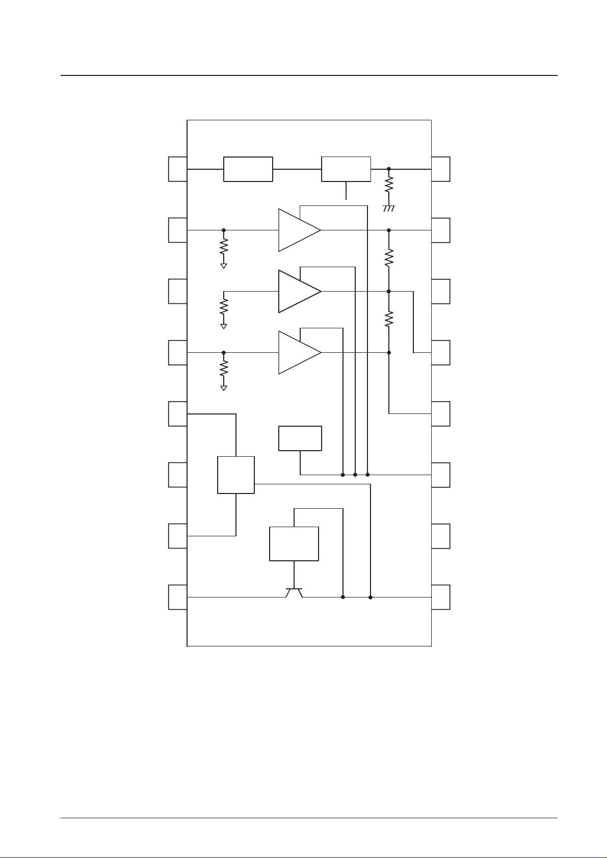
LA4801V
PW A
PW C
PW B
1
2
3
4
5
6
7
8
PW SW
16
9
15
14
13
12
11
10
MT SW
RIPPLE
FILTER
VREF
BIAS
PW SW
IN A
PWR C CONT
IN B
V
REF
PRE GND
V
REF
CONT
RF OUT
MUTE SW
OUT A
OUT C
OUT B
PWR GND
VCC 1
RF CONT
VCC 2
300kΩ
3kΩ
10kΩ
1kΩ
10kΩ
3kΩ
Top view
Pin Assignment and Block Diagram
 Loading...