SANYO LA4800V Datasheet

Ordering number: EN4335A
Monolithic Linear IC
LA4800V
3 V Stereo Headphone Power Amplifier
Overview
The LA4800V is a headphone stereo power amplifier IC that
features a high signal-to-noise ratio, high ripple rejection, low
distortion and low current consumption, making it ideal for
portable CD players.
Functions
.
Headphone stereo power amplifier
.
Beep tone
.
Power switch
.
Power mute switch
Features
.
96 dB (typ) high S/N ratio at 7 µV
.
76 dB (typ) high ripple rejection
.
0.07% (typ) low distortion with RL=16Ω
.
6.2 mA (typ) low current consumption
.
Outputs do not require electrolytic capacitors.
.
Available in 16-pin SSOPs
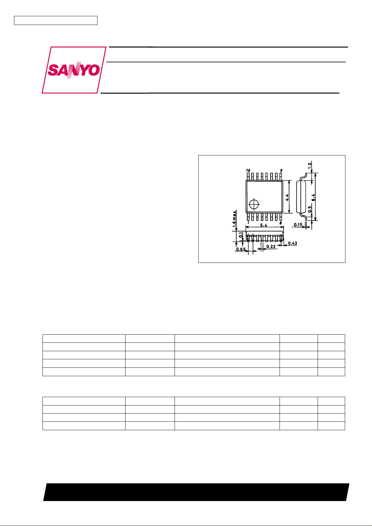
Package Dimensions
unit : mm
3178-SSOP16
[LA4800V]
SANYO : SSOP16
Specifications
Maximum Ratings at Ta = 25°C
Parameter Symbol Conditions Ratings Unit
Maximum supply voltage V
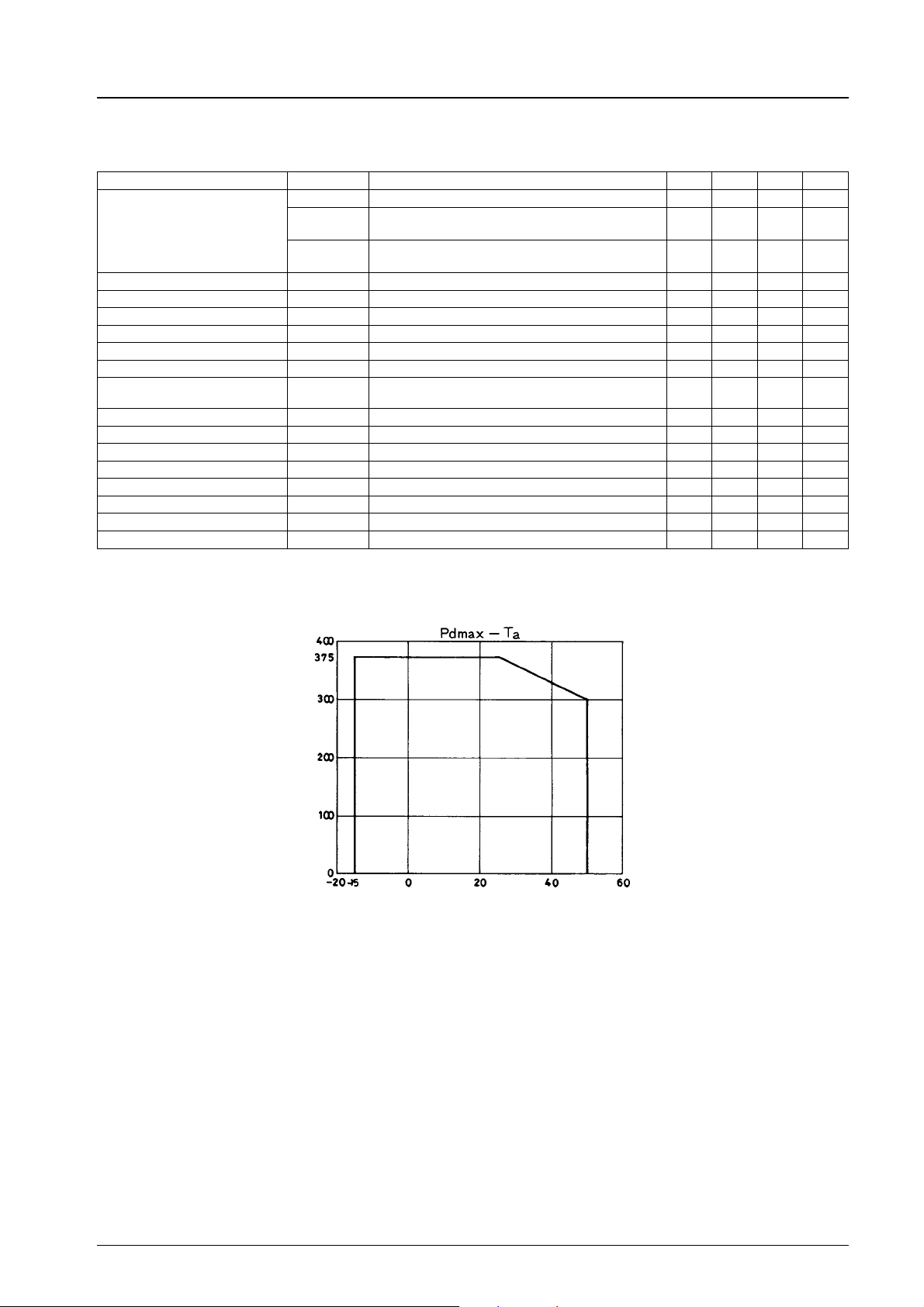
Power dissipation Pd max 375 mW
Operating temperature range Topr –15 to 50 °C
Storage temperature range Tstg –40 to 150 °C
Recommended Operating Ranges at Ta = 25°C
Parameter Symbol Conditions Ratings Unit
Supply voltage V
Load resistance R
Operating supply voltage range V
max 4.5 V
CC
CC
L
op 1.8 to 3.6 V
CC
3.0 V
16 to 32 Ω
SANYO Electric Co.,Ltd. Semiconductor Bussiness Headquarters
TOKYO OFFICE Tokyo Bldg., 1-10, 1 Chome, Ueno, Taito-ku, TOKYO, 110 JAPAN
32896HA(II)/60393TS No.4335-1/11

LA4800V
Operating Characteristics
at Ta = 25°C, VCC= 2.5 V, RL=16Ω,f=1kHzunless otherwise noted.
Values in parentheses indicate V
Parameter Symbol Conditions min typ max Unit
I
CCO1
I
Quiescent supply current
Voltage gain VG V
Channel balance V
Output power P
Total harmonic distortion THD V
Output noise voltage V
Crosstalk CT f = 1 kHz, TUN, V
Ripple rejection R.R
Mute attenuation V
Beep tone output voltage V
Output DC offset voltage V
Power ON current sensitivity l
Power OFF voltage sensitivity V
Mute OFF current sensitivity l
Mute OFF voltage sensitivity V
Mute ON voltage sensitivity V
CCO2
I
CCO3
RL
NO
OFF
O BEEPVI
DC OFFVI
1ON
1 OFF
16 OFF
16 OFFVCC
16 ON
IC OFF 0.05 1.0 µA
Mute ON
No input signal
= –10 dBm 10.3 11.8 13.3 dB
O
VO= –10 dBm –1 0 1 dB
VCC= 3.0 V, THD = 10% 15 25 mW
O
= 0.35 V 0.075 0.2 %
O
Rg=1kΩ, DIN AUDIO 7.8 15 µV
= 1.7 V, f = 100 Hz, VCR= –20 dBm,
V
CC
TUN = 100 Hz
THD = 1% –80 –96 dB
= –13.5 dBm (sine wave) 1.5 3.0 mV
=0V,Rg=1kΩ –20 0 20 mV
VCC= 1.7 V, V5^ 1.0 V 50 60 µA
VCC= 1.7 V, V5% 0.1 V 0.5 0.6 V
VCC= 1.7 V, V5^ 1.0 V 4.5 6.0 µA
= 1.7 V 1.0 1.25 1.5 V
VCC= 1.7 V 0.9 1.0 V
= 3.0 V
CC
1.6
6.2
3.0 mA
9.0 mA
(1.65)
(6.8)
= –10 dBm 35 45 dB
O
65 76 dB
Maximum power dissipation, Pd max − mW
Ambient temperature, Ta − °C
No.4335-2/11

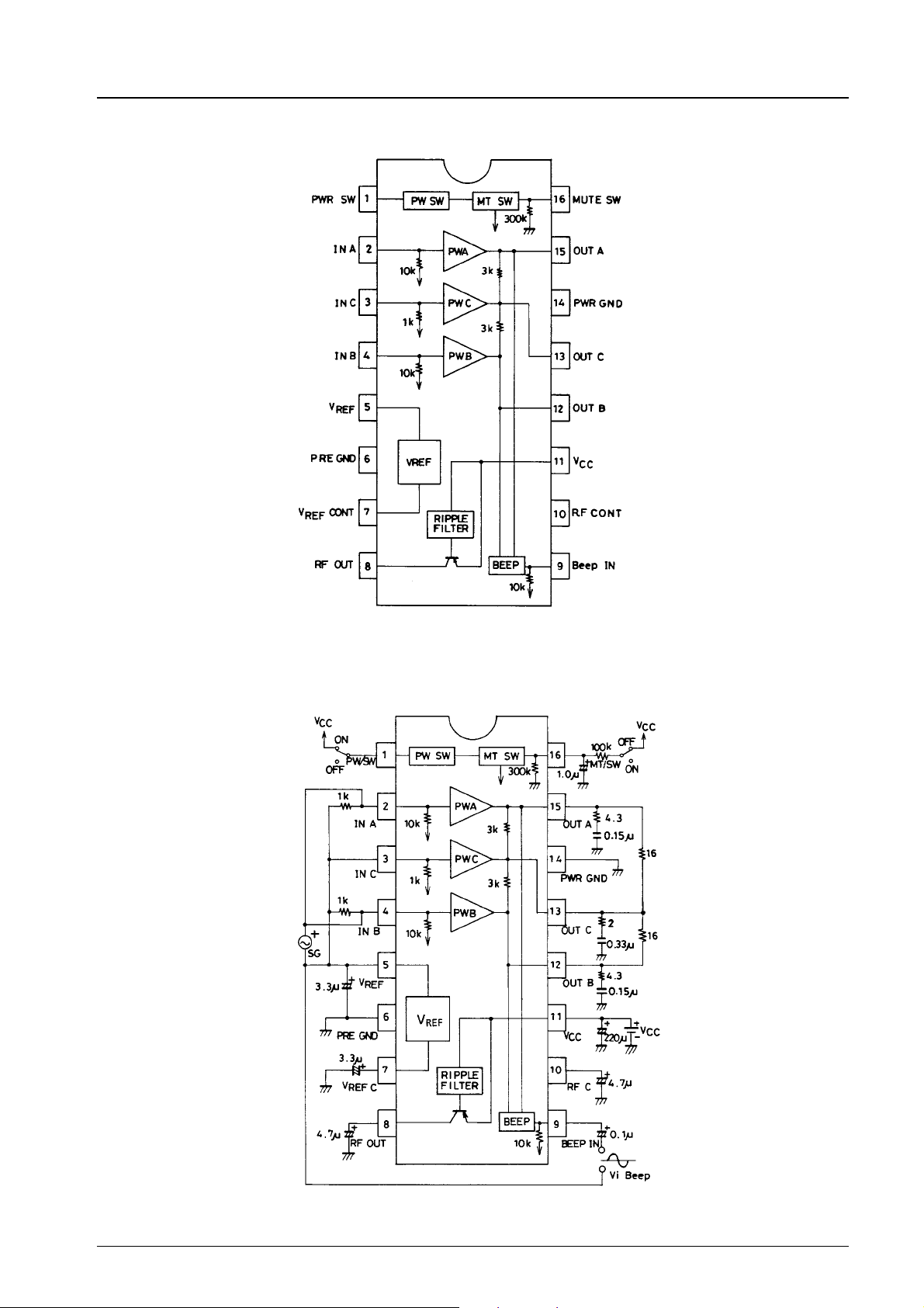
Pin Assignment and Block Diagram
LA4800V
Test Circuit
Top view
Unit (resistance: Ω)
Unit (resistance: Ω, capacitance: F)
No.4335-3/11

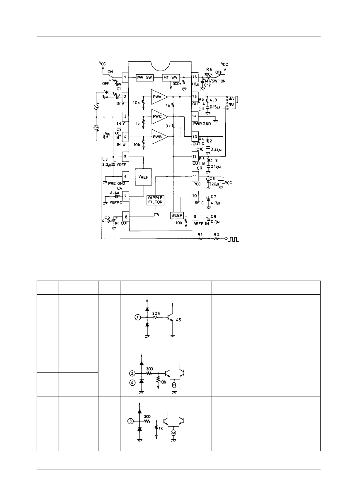
Sample Application Circuit
LA4800V
Pin Description
VCC= 2.5 V
Pin
number
1 PWR SW 0 to 0.7
2INA
4INB
Pin name V
Signal from microcontroller
Unit (resistance: Ω, capacitance: F)
Unit (resistance: Ω)
(V) Equivalent circuit Pin description
DC
Power switch
Turns ON the power to the V
1.1
Power input pins
10 kΩ input resistance
CC
pin.
3 IN C 1.1
Power amplifier common input pin
Usually connected to Vref
Continued on next page.
No.4335-4/11
 Loading...