

SANYO LA4742 Datasheet
Ordering number : ENN7043
92101TN (OT) No. 7043-1/9
Overview
The LA4742 is a 45 W 4-channel power amplifier IC for
car stereo systems. It features a built-in bridge circuit and
the ability to radically reduce the number of external
components required.
Features
• Maximum output power: 45 W × 4 channels
(VCC= 14.4 V, 4 Ω load, 1 kHz)
• 40 W × 4 channels (VCC= 13.7 V, 4 Ω load, 1 kHz)
• Requires only seven external components and does not
require an oscillation prevention RC circuit, a noise
filter, or a BS capacitor.
Functions
• Output offset detection function (DDL)
• Warning tone (beep) generation function
• Muting function
• Built-in standby switch
• Full complement of built-in protection circuits,
including protection from shorting to VCC, shorting to
ground, load shorting, overvoltages, and overheating.
• Maximum supply voltage before damage in the open
ground state: 16 V
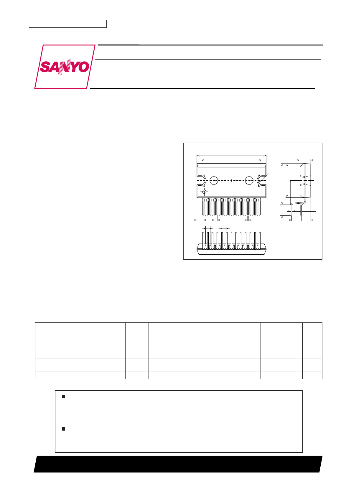
Package Dimensions
unit: mm
3236-HZIP25
2.02.0
29.2
2.60 (1.0)
25.6
0.53
R1.7
0.4
17.4
14.4
4.5
10.2
3.3
4.0
4.0
SANYO: HZIP25
[LA4742]
LA4742
SANYO Electric Co.,Ltd. Semiconductor Company
TOKYO OFFICE Tokyo Bldg., 1-10, 1 Chome, Ueno, Taito-ku, TOKYO, 110-8534 JAPAN
45 W Four-Channel (Bridge Circuit) Power Amplifier
Monolithic Linear IC
Any and all SANYO products described or contained herein do not have specifications that can handle
applications that require extremely high levels of reliability, such as life-support systems, aircraft’s
control systems, or other applications whose failure can be reasonably expected to result in serious
physical and/or material damage. Consult with your SANYO representative nearest you before using
any SANYO products described or contained herein in such applications.
SANYO assumes no responsibility for equipment failures that result from using products at values that
exceed, even momentarily, rated values (such as maximum ratings, operating condition ranges, or other
parameters) listed in products specifications of any and all SANYO products described or contained
herein.
Parameter Symbol Conditions Ratings Unit
Maximum supply voltage
V
CC
max1 Signal present 18 V
V
CC
max2 No signal (for 1 minute) 26 V
Maximum output current I
O
peak 4.5/ch A
Allowable power dissipation Pd max With an arbitrarily large heat sink 50 W
Operating temperature Topr –40 to +85 °C
Storage temperature Tstg –40 to +150 °C
Package thermal resistance θjc 1 °C/W
Specifications
Maximum Ratings at Ta = 25°C
No. 7043-2/9
LA4742
Parameter Symbol Conditions
Ratings
Unit
min typ max
Quiescent current I
CCORL
= ∞, Rg = 0 100 200 350 mA
Standby current Ist Vst = 0 V 10 µA
Output offset voltage V
N
offset Rg = 0 –100 +100 mV
Voltage gain VG V
O
= 0 dBm 25 26 27 dB
Voltage gain difference ∆VG –1 +1 dB
P
O
1 THD = 10 % 23 28 W
Output power P
O
max1 VCC= 13.7 V, VIN= 5 Vrms 40 W
P
O
max2 VIN= 5 Vrms 45 W
Total harmonic distortion THD P
O
= 4 W 0.05 0.4 %
Channel separation CHsep V
O
= 0 dBm, Rg = 10 kΩ 55 65 dB
Ripple rejection ratio SVRR f
r
= 100 Hz, VR= 0 dBm, Rg = 0 50 60 dB
Output noise voltage V
NO
Rg = 0, B.P.F. = 20 Hz to 20 kHz 100 200 µVrms
Muting attenuation Mute(att) V
O
= 20 dBm 70 80 dB
Operating Characteristics at Ta = 25°C, VCC= 14.4 V, f = 1 kHz, RL= 4 Ω, Rg = 600 Ω
Parameter Symbol Conditions Ratings Unit
Recommended supply voltage V
CC
14.4 V
Recommended load resistance R
L
4 Ω
Operating supply voltage range V
CC
op 9 to 18 V
Operating Conditions at Ta = 25°C
No. 7043-3/9
LA4742
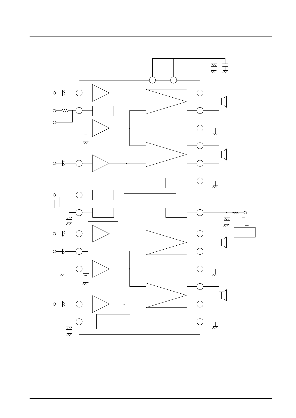
Sample Application Circuit and Block Diagram
911
6 20
725
8
5
312
2
4
2210
1715
191
1813
21
2314
2416
Top view
OUT 1+
VCC1/2 VCC3/4
OUT 1–
PWR GND 1
OUT 2+
OUT 2–
PWR GND 2
Mute
OUT 3+
OUT 3–
PWR GND 3
10kΩ
OUT 4+
OUT 4–
PWR GND 4
+
+
+
+
+
+
+
+
+
IN 1
CLIP DET
0.22µF
IN 2
0.22µF
3.3µF
0.022µF
IN 3
ST BY
0.22µF
AUX IN
0.22µF
IN 4
0.22µF
47µF
R.F
2200µF
22µF
PRE GND
ON TIME C
+5V
Protective
Circuit
Stand by
Switch
Clip Detect
Circuit
Ripple
Filter
Mute
Circuit
Aux
Circuit
Low Level
Mute ON
Muting &
ON Time Control
Circuit
Protective
Circuit
–
–
+
+
+
–
–
+
+
–
–
+
+
+
–
–
A13765
+5V
ST ON
10kΩ
 Loading...