

SANYO LA4725 Datasheet
Ordering number : EN*5715
Preliminary
Monolithic Linear IC
LA4725
2-Channel BTL Power Amplifier (30 W+30 W)
with Standby Switch for Car Stereos
Overview
The LA4725 is a BTL two-channel power IC for car
audios developed in pursuit of excellent sound quality.
Low-region frequency characteristics have been improved
through the use of a new NF capacitorless circuit, and
crosstalk which causes “muddy” sound has been reduced
by improving both circuit and pattern layout. As a result
the LA4725 provides powerful bass and clear treble.
Features
⋅ High power: supports total output of 30 W+30 W. [EIAJ
power] (V
=14.4 V, THD=30 %, RL=4 Ω)
CC
⋅ Less pop noise.
⋅ Designed for excellent sound quality.
(fL<10 Hz, fH=130 kHz)
⋅ Any rise time settable by an external capacitor.
⋅ Standby switch circuit on chip. (microcontroller support-
ed)
⋅ Various protectors on chip.
(output-to-ground short/ output-to-VCC short/ load
short/ overvoltage/ thermal shutdown circuit)
⋅ The LA4725 is pin-compatible with the LA4728.
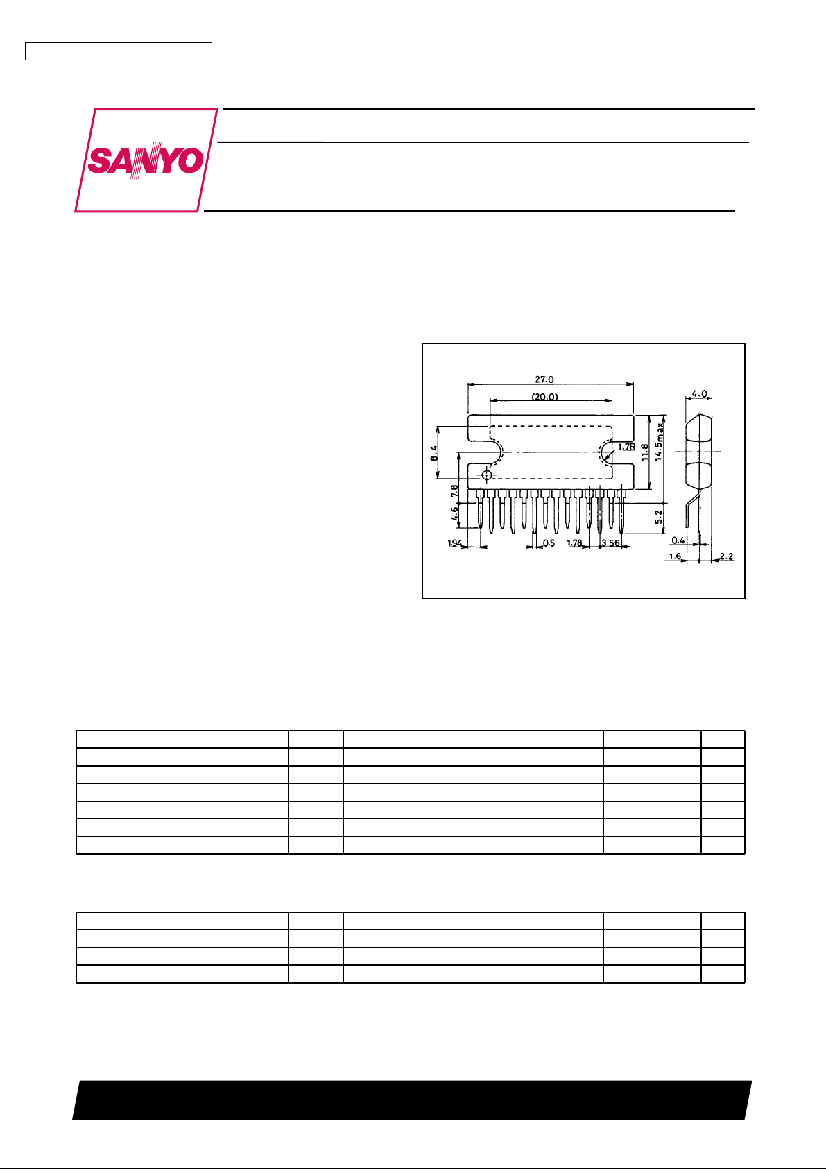
Package Dimensions
unit: mm
3113A-SIP14HZ
[LA4725]
SANYO: SIP14HZ
Specifications
Maximum Ratings at Ta = 25 ˚C
Parameter Symbol Conditions Ratings Unit
Maximum supply voltage V
Surge supply voltage V
Maximum output current I
Allowable power disspation Pd max With arbitrarily large heat sink 32 W
Operating temperature Topr –35 to +85 ˚C
Storage temperature Tstg –40 to +150 ˚C
Recommended Conditions at Ta = 25 ˚C
Parameter Symbol Conditions Ratings Unit
Recommended supply voltage V
Operating voltage range V
Recommended load resistance R
max 18 V
CC
surge f ≤ 0.2 s, single giant pulse 50 V
CC
peak Per channel 3.0 A
O
CC
op Range where Pd max is not exceeded 9 to 16 V
CC
op 4 Ω
L
13.2 V
SANYO Electric Co.,Ltd. Semiconductor Bussiness Headquarters
TOKYO OFFICE Tokyo Bldg., 1-10, 1 Chome, Ueno, Taito-ku, TOKYO, 110 JAPAN
32497RM(KOTO) No.5715-1/3
LA4725
Operating Characteristics at Ta = 25 ˚C, VCC = 13.2 V, RL = 4 kΩ, f = 1 kHz, Rg = 600 Ω
Parameter Symbol Conditions
Quiescent current I
Standby current I
Voltage gain VG 38 40 42 dB
Total harmonic distortion THD P
Output power
Output offset voltage V
Output noise voltage V
Ripple rejection ratio SVRR Rg=0, f
Channel separation Chsep Rg=10 kΩ, V
Input resistance Ri 21 30 39 kΩ
Standby pin applied voltage Vst Amp on, applied through 10 kΩ 2.5 V
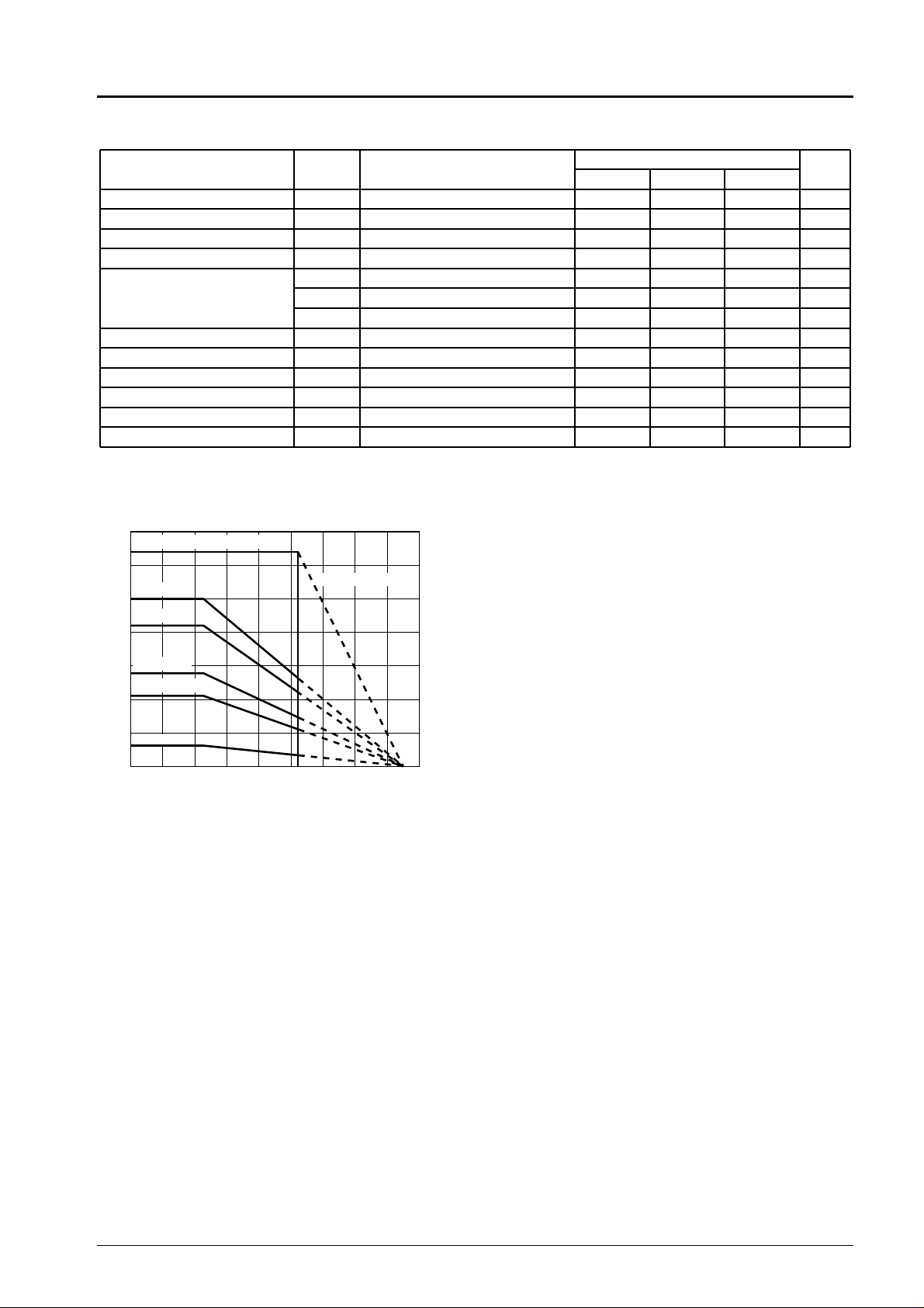
35
Arbitrarily large heat sink
32
30
θf=3˚C/W
25
θf=4˚C/W
20.8
20
Pd max — Ta
N offset
Rg=0 70 125 250 mA
CCO
ST
=1 W 0.06 0.2 %
O
RL=4 Ω, THD=10 %, VCC=13.2 V 13 17 W
P
O1
P
RL=4 Ω, THD=10 %, VCC=14.4 V 20 W
O2
P
RL=4 Ω, THD=30 %, VCC=14.4 V 30 W
O3
Rg=0 –300 +300 mV
Rg=0, B.P.F.=20 Hz to 20 kHz 0.1 0.5 mVrms
NO
=100 Hz, VR=0 dBm 40 50 dB
R
=0 dBm 50 60 dB
O
θjc=2.0˚C/W
min typ max
Ratings
10 60 µA
CC
Unit
V
15
θf=7˚C/W
13.9
θf=10˚C/W
10.4
10
5
No fin
3.1
Allowable power dissipation, Pd max — W
0
–20 0 20 40 140 16060 80 100 120
Ambient temperature, Ta — ˚C
No.5715-2/3
 Loading...