

Page 1
Ordering number : ENA0508
Monolithic Linear IC
LA47202P
Four-Channel BTL Power
Amplifier for Car Audio Systems
Overview
The LA47202P is a 4-channel BTL power amplifier IC developed for use in car audio applications. The LA47202P adopts
a pure complementary output stage circuit structure with a v-pnp transistor for the high side and an npn transistor for the
low side to provide both high output power and high quality sound.
The LA47202P integrates all the functions required for car audio applications on the same chip, including a standby switch,
a muting function, and a full complement of protection circuits. It also features a self diagnostics function.
Functions
• High output : PO max = 47W (typ.) (VCC = 14.4V, f = 1kHz, JEITA max, RL = 4Ω)
: PO max = 29W (typ.) (VCC = 14.4V, f = 1kHz, THD = 10%, RL = 4Ω)
: PO max = 22W (typ.) (VCC = 14.4V, f = 1kHz, THD = 1%, RL = 4Ω)
• Muting function incorporated (pin 22)
• Built-in standby switch (pin 4)
• Self diagnostics function incorporated (pin 25) :
Output of both output offset det ect i on, shorting to VCC or ground and load shorting signals
• Electric mirror noise decrease
• Full compliment of protection circuits (shorting to VCC, shorting to ground, load shorting, overvoltage, and thermal
protection).
• Improved oscillation stability
Note 1 : Take care to avoid w ron g con necti on . Othe rwi se, IC or e qui pm ent ma y suffer bre akd own , dam age, or det eri ora t ion.
Note 2 : The protective circuit fu nctio n is t o avoi d the a b norm al state (wr ong con nection of t he out put ) tem pora ril y and does
not guarantee that IC is not broken.
These protective functions do not operate outside the ope r a ti on guarantee range, and wrong connection of output
may cause breakdown of IC.
Note 3 : External parts, such as the anti-oscillation part, diode to prevent breakdown, may become necessary depending on t he
set condition. Check their necessity for each set.
Any and all SANYO Semiconductor products described or contained herein do not have specifications
that can handle applications that require extremely high levels of reliability, such as life-support systems,
aircraft's control systems, or other applications whose failure can be reasonably expected to result in
serious physical and/or material damage. Consult with your SANYO Semiconductor representative
nearest you before using any SANYO Semiconductor products described or contained herein in such
applications.
SANYO Semiconductor assumes no responsibility for equipment failures that result from using products
at values that exceed, even momentarily, rated values ( such as maximum ratings, operating condition
ranges, or other parameters) listed in products specifications of any and all SANYO Semiconductor
products described or contained herein.
D2706 MS PC 20060809-S00002 No.A0508-1/8
Page 2
LA47202P
Specifications
Maximum Ratings at Ta = 25°C
Parameter Symbol Conditions Ratings Unit
V
max1 Without signal, t = 1 minute 26 V Maximum supply voltage
CC
V
max2 When operating 18 V
CC
Maximum output current IO peak Per channel 4.5 A
Allowable power dissipation Pd max W ith an iInfinitely large heat sink 50 W
Operating temperature Topr -40 to +85 °C
Storage temperature Tstg -40 to +150 °C
Thermal resistance between
junction cases
Note) The relationship between the power dissipation (Pd) and the junction-to-case thermal resistance (θj-c), heat sink
thermal resistance (θf) and junction temperature (Tj), case temperature (Tc), and ambient temperature (Ta) is as
expressed by the following equation :
Tj = Pd (θj-c+θf) +Ta
= Pd×θj-c+Tc, *Tc = Pd×θf+Ta
Note that Tj max must be limited with Tstg max (150°C).
Recommended Operating Ranges
Parameter Symbol Conditions Ratings Unit
Recommended supply voltage VCC 14.4 V
Recommended load resistance RL 4 Ω
Operating supply voltage range VCC op Range not exceceeding Pd max 9 to 16 V
Electrical Characteristics at Ta = 25°C, VCC = 14.4V, RL = 4Ω, f = 1kHz, Rg = 600Ω
Parameter Symbol Conditions
Quiescent current I
Standby current Ist Vst = 0V 10 µA
Voltage gain VG VO = 0dBm 25 26 27 dB
Voltage gain difference ∆VG -1 +1 dB
Output power
Output offset voltage Vnoffset Rg = 0 -150 +150 mV
Total harmonic distortion THD PO = 4W 0.05 0.3 %
Channel separation CHsep VO = 0dBm, Rg = 10kΩ 55 65 dB
Ripple rejection ratio SVRR Rg = 0, fr = 100Hz, VCCR = 0dBm 45 60 dB
Output noise voltage VNO Rg = 0, BPF = 20Hz to 20kHz 100 200 µVrms
Input resistance Ri 50 kΩ
Mute attenuation Matt VO = 20dBm, mute : on 65 80 dB
* 0dBm = 0.775Vrms
θj-c 1 °C/W
at Ta = 25°C
Ratings
min typ max
RL = ∞, Rg = 0 200 400 mA
CCO
PO THD = 10% 24 29 W
PO max1 VCC = 13.7V, JEITA max 42 W
PO max2 JEITA max 47 W
Unit
No.A0508-2/8
Page 3
LA47202P
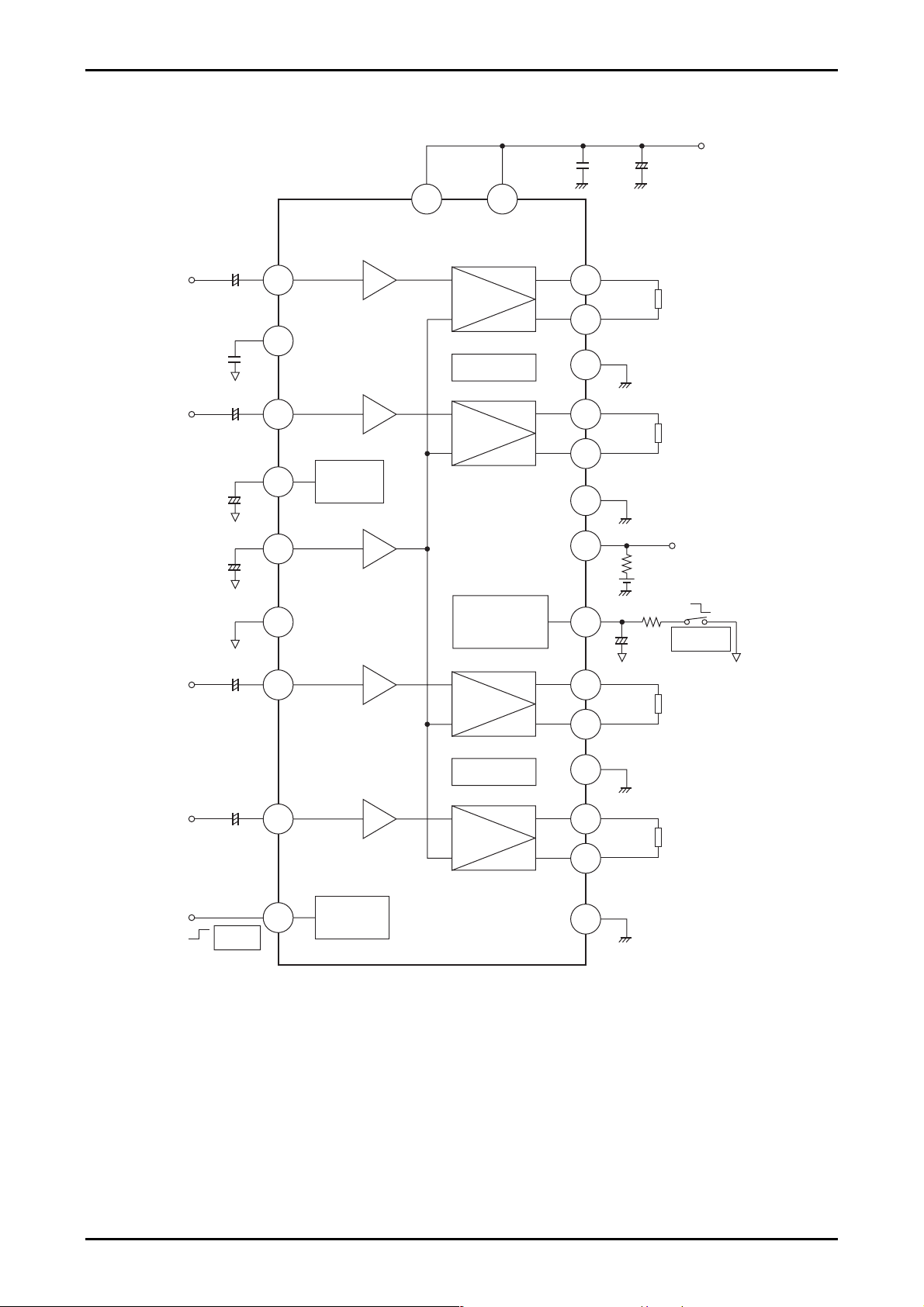
Block Diagram
6 20
VCC3/4VCC1/2
0.1µF
+
2200µF
4700pF
IN 1
+
0.47µF
CONTROL
IN 2
+
0.47µF
DC
+
22µF
11 9
1
12
10
Ripple
filter
+
-
Protective
+
-
+
-
circuit
+
-
OUT 1+
OUT 1-
7
PWR GND1
8
OUT 2+
5
OUT 2-
3
PWR GND2
2
AC GND
0.47µF
PRE GND
+
IN 3
+
0.47µF
IN 4
+
0.47µF
16
Mute
circuit
15 17
14
+
-
Protective
++
-
+
-
circuit
-
25
2213
19
18
21
23
4.7kΩ
5V
10kΩ
Mute
+
1µF
OUT 3+
OUT 3-
PWR GND3
OUT 4+
OUT 4-
STBY
+5V
ST ON
4
Standby
switch
PWR GND4
24
The components and constant values in the test circuit are used for confirmation of characteristics and do not guarantee
that the application equipment will be free from malfunction or trouble.
R
L
R
L
OFFSET
DIAG
Low Level
Mute ON
R
L
R
L
V
CC
No.A0508-3/8
Page 4

LA47202P
Description of Operation
1. Standby switch function (pin 4)
The pin 4 threshold voltage is set to about 3 VBE.
The amplifier is turned ON at the application voltage of 3.0V or more and OFF at 0.5V or less.
2. Muting function (pin 22)
When pin 22 is set to the ground potential, the LA47202P goes to the muted state. This supports implementation of an
audio muting function.
The muting function is turned on when a level of 1V or lower is applied through a 10kΩ resistor, and the function is
turned off when this pin is open.
The muting time constant can be set with an external RC circuit.
3. Self diagnostics function (pin 25)
This function detects abnormal IC states, and outputs a signal from pin 25. Applications can prevent damage to
speakers and other problems by using a microcontroller to detect the pin 25 signal and control the standby switch
accordingly.
(1) Output short-circuit to VCC/ground : Pin 25 becomes LOW.
(2) Load short-circuit : Pin 25 repeats HIGH and LOW states according to the output signal.
(3) Output offset abnormality : Pin 25 goes low if the OUT pin (VN) voltage becomes lower than the
detection level. Problems that can cause an output offset abnormality
include input capacitor leakage and half shorts between the input pins and
adjacent circuit components.
Note that pin 25 is the NPN open collector output (active low). Keep pin 25 open-connection when not using.
4. CONTROL pin (pin 1)
The protective circuit response speed is adjusted by the pin 1 capacitor.
By adjusting the response speed of the protective circuit, abnormal sound generated when the protective circuit
operates at input of the large signal can be prevented.
When the capacitance value increases, abnormal sound is more difficult to be generated, but the response speed of the
protective circuit becomes lower. The capacitance value must be limited to maximum 0.01µF. The recommended
value is 4700pF.
Check the optimum value for each set.
As this is designed so that the protective circuit is activated when pin 1 has the GND potential, the protective circuit
becomes normally active when the capacitor is short-circuited.
5. AC GND pin (pin 16)
Be sure to use the pin 16 capacitor with the capacity the same as that of the input capacitor and connect it to PREGND
the same as that of the input capacitor.
6. Sound quality (low frequencies)
The frequency characteristics i n l ow fre que ncy ra nge m a y b e im prove d by varyi ng the cap acita nce of inp ut ca pacitor .
Note that this may cause influence on the shock noise, carry out confirmation with each set before varying the
capacitance value.
7. Impulse noise related systems
While the LA47202P does include an impulse noise prevention circuit, we recommend using the muting function
together with this circuit.
• When the amplifier is ON, turn ON the muting function simultaneously with power ON. When the output DC
potential has stabilized, turn OFF the muting function.
• When turning OFF the amplifier, first turn ON the muting function, then turn OFF power supply.
No.A0508-4/8
Page 5

LA47202P
8. Oscillation stability
Pay due attention on the following points because parasitic oscillation may occur due to effects of the capacity load,
board layout, etc.
(1) Capacity load
When the capacitor is to be inserted between each output pin and GND so as to prevent electric m irror noise, select
the capacitance of maximum 1200pF. (Conditions : Our recommended board, RL = 4Ω)
(2) Board layout
• Provide the VCC capacitor of 0.1µF in the position nearest to IC.
• PREGND must be independently wired a nd connected to the GND point that is as stable as possible, suc h as the
minus pin of the 2200µF VCC capacitor.
In case of occurrence of parasitic oscillation, any one of following parts may be added as a countermeasure.
Note that the optimum capacitance must be checked for each set in the mounted state.
• Series connection of CR (0.1µF and 2.2Ω) between BTL outputs
• Series connection of CR (0.1µF and 2.2Ω) between each output pin and GND.
Package Dimensions
unit : mm (typ)
3236A
(5.0)
(12.3)
125
(2.6)
2.0
(8.5)
(1.0)
29.2
25.6
(22.8)
( 2.5)
2.0
0.52
(R1.7)
(14.4)
18.6 max
21.7
3.5
SANYO : HZIP25
70
4.5
(11.0)
0.4
4.0
14.5
4.2
60
Infinite heat sink θj-c=1°C/W
50
40
heat sink(θf=3.5°C/W)
θj-c+θf=4.5°C/W
30
20
10
No heat sink θj-a=39°C/W
Maximum power dissipation, Pd max -- W
0
-40 -20 0 20 40 60 80 100 120 140 160
Pd max -- Ta
Ambient temperature, Ta -- °C
No.A0508-5/8
Page 6

LA47202P
250
RL = Open
I
CCO
-- V
CC
Rg = 0Ω
200
mA
--
CCO
150
100
50
Quiescent current, I
0
414121086161820
50
f = 1kHz
Supply voltage, V
P
-- V
O
CC --
CC
V
RL = 4Ω
THD = 10%
40
W
-O
30
20
12
RL = Open
N
CC
V
-- V
Rg = 0Ω
10
V
-N
8
6
4
2
Output midpoint voltage, V
0
414121086161820
Supply voltage, V
P
-- f
25
20
W
-O
15
10
O
CC --
V
Output power, P
10
Output power, P
5
VCC = 14.4V
RL = 4Ω
0
8141512 1310 11916177
10
1.0
0.1
Total harmonic distortion, THD -- %
0.01
VCC = 14.4V
7
5
RL = 4Ω
f = 1kHz
3
2
7
5
3
2
7
5
3
2
0.1
Supply voltage, V
THD -- P
CH2
7
35273527352
1.0
CH4
CH1
CC --
O
V
CH3
10
100
Output power, PO -- W
10
1.0
0.1
Total harmonic distortion, THD -- %
0.01
VCC = 14.4V
7
RL = 4Ω
5
f = 10kHz
3
2
7
5
3
CH1
2
7
CH4
5
3
2
0.1
THD -- P
CH3
CH2
7
35273527
1.0
O
352 7
10
100
Output power, PO -- W
THD = 1%
0
3527
10 100k
3527
100
352735218
1k
Frequency, f -- Hz
10
VCC = 14.4V
7
5
RL = 4Ω
f = 100Hz
3
2
1.0
7
5
3
2
0.1
7
5
3
Total harmonic distortion, THD -- %
2
0.01
0.1 100
35273527
THD -- P
7
1.0
CH4
352
O
CH2
CH1
Output power, PO -- W
1.0
VCC = 14.4V
7
5
RL = 4Ω
PO = 4W
3
2
0.1
7
CH4
5
3
2
0.01
7
5
3
Total harmonic distortion, THD -- %
2
0.001
100 100k
CH2
CH1
CH3
3527
THD -- f
1k
35 75232
Frequency, f -- Hz
10k
CH3
10
10k
No.A0508-6/8
Page 7

LA47202P
1
0
--1
Response -- dB
--2
Response -- f
VCC = 14.4V
RL = 4Ω
VO = 0dBm
150
mVrms
--
100
NO
50
V
NO
-- Rg
VCC = 14.4V
RL = 4Ω
Output noise voltage, V
--3
10
7532
100
7532
1k
75327532
10k 100k
Frequency, f -- Hz
80
70
60
50
CH. Separation -- f
CH1→3
CH1→4
CH1→2
0
10
7532
100
7532
1k
75327532
10k 100k
Rg -- V
80
70
60
50
CH. Separation -- f
CH2→3
CH2→4
CH2→1
Channel separation -- dB
Channel separation -- dB
40
VCC = 14.4V
RL = 4Ω
30
Rg = 10kΩ
VO = 0dBm
(CH1→)
20
10
7
3527
3527
100
Frequency, f -- Hz
80
70
60
50
40
VCC = 14.4V
RL = 4Ω
30
Rg = 10kΩ
CH. Separation -- f
VO = 0dBm
(CH3→)
20
10
7
3527
3527
100
1k
Frequency, f -- Hz
80
SVRR -- V
40
VCC = 14.4V
Channel separation -- dB
RL = 4Ω
30
Rg = 10kΩ
VO = 0dBm
(CH2→)
35273527
1k
10k
100k
20
3527
10 100k
3527
100
1k
3527352
Frequency, f -- Hz
CH. Separation -- f
CH4→1
CH3→2
CH3→2
CH3→4
80
70
60
50
40
Channel separation -- dB
30
VCC = 14.4V
RL = 4Ω
Rg = 10kΩ
VO = 0dBm
(CH4→)
35273527
10k
100k
20
3527
10 100k
3527
100
1k
3527352
Frequency, f -- Hz
CC
80
SVRR -- f
R
10k
CH4→3
CH4→2
10k
70
60
VCCR = 0dBm
50
fR = 100Hz
Rg = 0Ω
Ripple rejection ratio, SVRR -- dB
RL = 4Ω
CVCC = 0.1µF
40
810121416
Supply voltage, V
CC --
V
CH2
70
CH4
60
50
Ripple rejection ratio, SVRR -- dB
40
10 100k
CH3
CH1
VCC = 14.4V
VCCR = 0dBm
Rg = 0Ω
RL = 4Ω
CVCC = 0.1µF
100 10k1k
Ripple frequency, fR -- Hz
753275327532753218
No.A0508-7/8
Page 8

LA47202P
80
70
60
SVRR -- VCCR
CH2
CH4
CH3
CH1
60
50
40
30
f = 1kHz
RL = 4Ω
Pd -- P
VCC = 16V
O
VCC = 14.4V
20
Power dissipation, Pd -- W
10
50
Ripple rejection ratio, SVRR -- dB
VCC = 14.4V
fR = 100Hz
Rg = 0Ω
RL = 4Ω
CVCC = 0.1µF
40
0 1.0 1.50.5 2.0
SVRR = 20log (VCCR / VO)
Supply ripple voltage, VCCR -- Vrms
10
RL = 4Ω
Offset DIAG -- V
CC
0
0.1
7532
1.0 10
Output power, PO -- W
Pd = VCC×ICC-4P
77553232
O
100
Rg = 0Ω
8
6
4
1/2 V
CC
Offset DIAG -- V
2
Detection Level
0
812141610 18
Supply voltage, V
CC --
V
Specifications ofany and allSANYO Semiconductor products described or contained herein stipulate the
performance, characteristics, and functions of the described products in the independent state, and are
not guarantees of the performance, characteristics, and functions of the described products as mounted
in the customer's products or equipment. To verify symptoms and states that cannot be evaluated in an
independent device, the customer should always evaluate and test devices mounted in the customer's
products or equipment.
SANYO S emiconductor Co., Ltd. strives to supply high-quality high-reliability products. H owever, any
and all semiconductor products fail with some probability. It is possible that these probabilistic failures
could give rise to accidents or events that could endanger human lives, that could give rise to smoke or
fire, or that could cause damage to other property. When designing equipment, adopt safety measures
so that these kinds of accidents or events cannot occur. Such m easures include but are not limited to
protective circuits and error prevention circuits for safe design, redundant design, and structural design.
In the event that any or all SANYO Semiconductor products (including technical data,services) described
or contained herein are controlled under any of applicable local export control laws and regulations, such
products must not be exported without obtaining the export license from the authorities concerned in
accordance with the above law.
No part of this publication may be reproduced or transmitted in any fo rm or by any means, electronic or
mechanical, including photocopying and recording, or any information storage or retrieval system, or
otherwise, without the prior written permission of SANYO Semiconductor Co., Ltd.
Any and all information described or contained herein are subject to change without notice due to
product/technology improvement, etc. When designing equipment, refer to the "Delivery Specification"
for the SANYO Semiconductor product that you intend to use.
Information (including circuit diagrams and circuit parameters) herein is for example only; it is not
guaranteed for volume production. SANY O Semiconductor believes information herein is accurate and
reliable, but no guarantees are made or implied regarding its use or any infringements of intellectual
property rights or other rights of third parties.
This catalog provides information as of December, 2006. Specifications and information herein are subject
to change without notice.
PS No.A0508-8/8
 Loading...