

SANYO LA4708 Datasheet
Ordering number: EN5245A
Monolithic Linear IC
LA4708
20 W 2-channel BTL AF Power Amplifier
for Car Stereos
Overview
The LA4708 is a BTL two-channel power IC for car audio
developed in pursuit of excellent sound quality. Low-region
frequency characteristics have been improved through the use
of a new NF capacitorless circuit, and crosstalk which causes
‘‘muddy’’ sound has been reduced by improving both circuit
and pattern layout. As a result, the LA4708 provides powerful
bass and clear treble. In addition, the LA4708 features on-chip
protectors and standby switch. The LA4708 is also
pin-compatible with the LA4705NA (car stereo-use 17 W
two-channel power IC), and can be substituted for the
LA4705NA for higher power. (When the board is shared, pins
1 and 9 must be left open.)
Features
.
High power: supports total output of 30 W + 30 W
(V
= 13.2 V, THD = 30%, RL=4Ω)
CC
.
Supports RL=2Ω(PO= 30 W when VCC= 13.2 V,
THD = 10%)
.
Designed for excellent sound quality
(f
< 10 Hz, fH= 130 kHz)
L
.
NF capacitorless
.
Any on time settable by external capacitor
.
Less pop noise
.
Standby switch circuit on chip (microprocessor supported)
.
Various protectors on chip
(output-to-ground short/output-to-V
load short/overvoltage/thermal shutdown circuit)
CC
short/
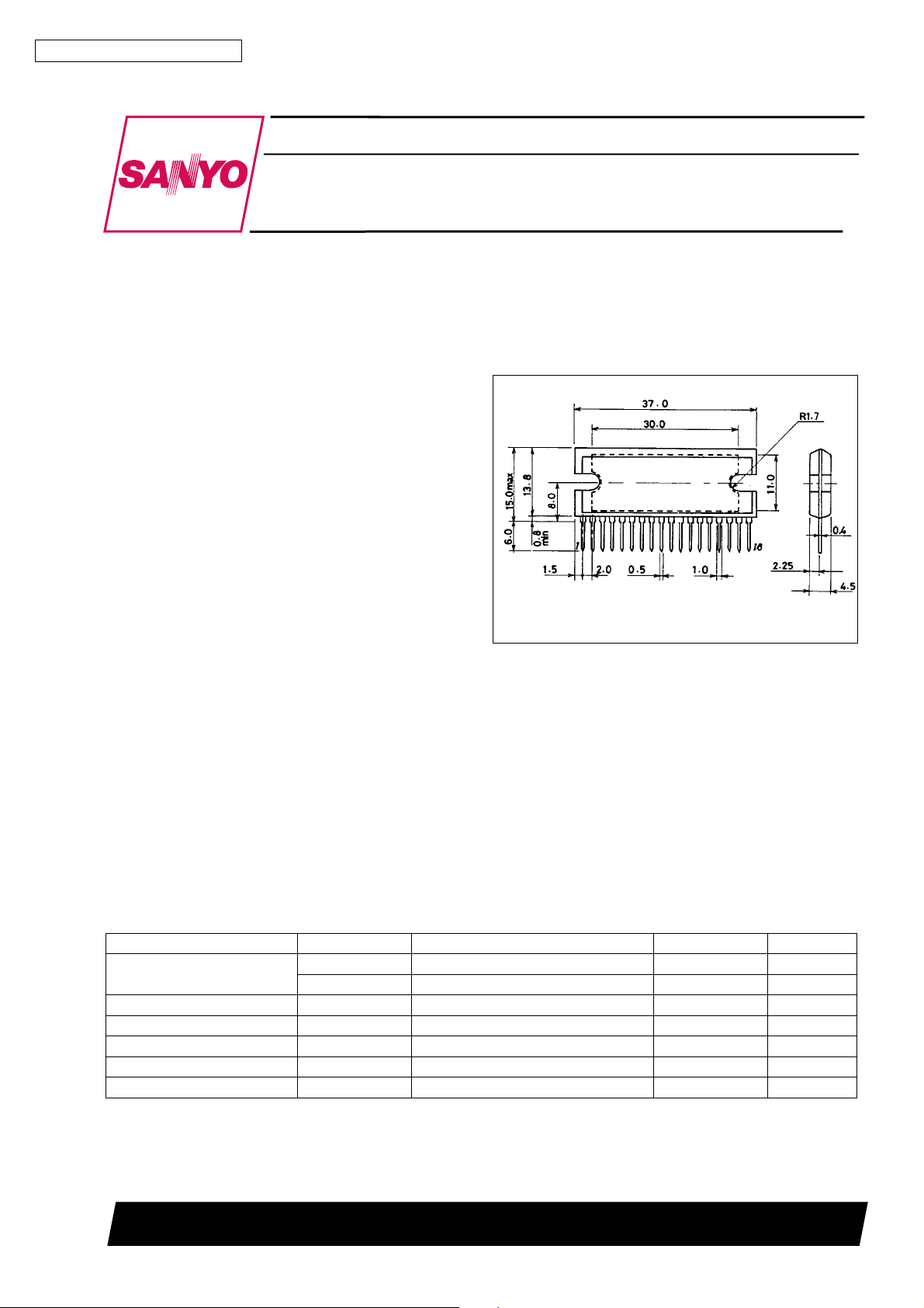
Package Dimensions
unit: mm
3109-SIP18H
[LA4708]
SANYO : SIP18H
Specifications
Maximum Ratings at Ta = 25°C
Parameter Symbol Conditions Ratings Unit
Maximum supply voltage V
Surge supply voltage V
Maximum output current I
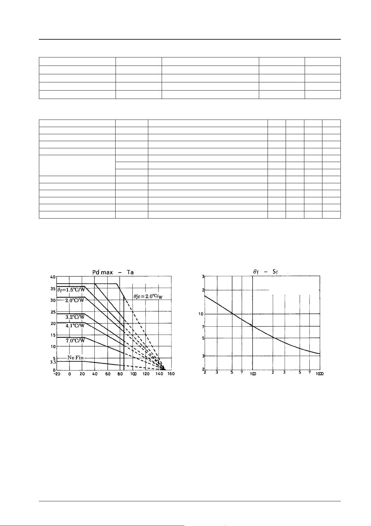
Allowable power dissipation Pd max Arbitrarily large heat sink 37.5 W
Operating temperature Topr –35 to +85 °C
Storage temperature Tstg –40 to +150 °C
* Set VCC,RLin a range that does not exceed Pd max = 37.5 W
max 1 No signal,t=60s 24 V
CC
V
max 2 16 V
CC
surge t % 0.2 s, single giant pulse 50 V
CC
peak Per channel 4.5 A
O
SANYO Electric Co.,Ltd. Semiconductor Bussiness Headquarters
TOKYO OFFICE Tokyo Bldg., 1-10, 1 Chome, Ueno, Taito-ku, TOKYO, 110 JAPAN
93096HA(II)/13096HA(II) No.5245-1/9
LA4708
Operating Conditions at Ta = 25°C
Parameter Symbol Conditions Ratings Unit
Recommended supply voltage V
Operating voltage range V
Recommended load resistance R
Recommended load resistance range
CC
op Range where Pd max is not exceeded 9 to 16 V
CC
L
RLop 2to4 Ω
Operating Characteristics at Ta = 25°C, VCC= 13.2 V, RL=4Ω,f=1kHz, Rg = 600 Ω
Parameter Symbol Conditions min typ max Unit
Quiescent current I
Standby current Ist 10 60 µA
Voltage gain VG 38 40 42 dB
Total harmonic distortion THD P
Output power
Output offset voltage V
Output noise voltage V
Ripple rejection ratio SVRR Rg = 0, f
Channel separation CHsep Rg = 10 kΩ,V
Input resistance r
Standby pin applied voltage Vst Amp on, applied through 10 kΩ 2.5 V
CCO
= 2 W 0.07 0.4 %
1 THD = 10% 16 20 W
P
O
P
2 THD = 10%, VCC= 14.4 V 24 W
O
P
3 THD = 10%, RL=2Ω 30 W
O
offset Rg = 0 –300 +300 mV
N
NO
i
O
Rg = 0, B.P.F. = 20 Hz to 20 kHz 0.1 0.5 mVrms
= 100 Hz, VR= 0 dBm 40 50 dB
R
= 0 dBm 50 60 dB
O
13.2 V
4 Ω
70 150 250 mA
21 30 39 kΩ
CC
V
Allowable power dissipation, Pd max — W
Arbitrarily large heat sink
Ambient temperature, Ta — °C
— °C/W
f
Heat sink thermal resistance, θ
Al heat sink, t = 1.5 mm
Tightening torque 39 Nccm
With silicone grease applied
Heat sink area, Sf—cm
2
No.5245 -2/9
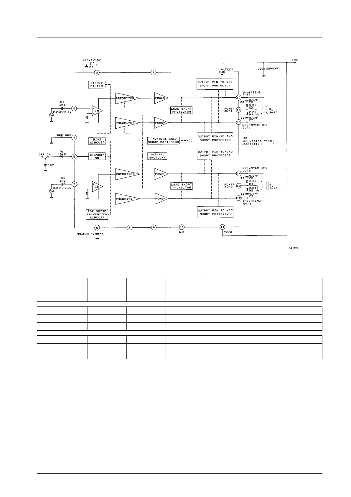
Equivalent Circuit Block Diagram
LA4708
--
--
Pins 1,9 : Don’t use
Pin 10 : No connection
Each Pin Voltage
VCC= 13.2 V, 5 V applied through STBY = 10 kΩ,RL=4Ω,Rg=0
PinNo.123456
Name IN1 DC Pre-GND STBY ON TIME
Pin voltage (V) 0.29 1.58 6.55 0 3.2 2.28
Pin No. 7 8 9 10 11 12
Name IN2 POP – N.C V
Pin voltage (V) 1.58 2.08 0.29 0 13.2 6.5
Pin No. 13 14 15 16 17 18
Name PWR–GND 2 +OUT 2 +OUT 1 PWR–GND 1 –OUT 1 V
Pin voltage (V) 0 6.5 6.5 0 6.5 13.2
2 –OUT 2
CC
CC
1
No.5245 -3/9
 Loading...