

SANYO LA4705 Datasheet
Ordering number: EN3848D
Monolithic Linear IC
LA4705
15 W 2-channel BTL AF Power Amplifier
for Car Stereos
Overview
The LA4705 is a BTL two-channel power IC for car audio and
radio-cassette players developed in pursuit of excellent sound
quality. Low-region frequency characteristics have been
improved through the use of a new NF capacitorless circuit,
and crosstalk which causes ‘‘muddy’’ sound has been reduced
by improving both circuit and pattern layout. As a result, the
LA4705 provides powerful bass and clear treble. In addition,
the LA4705 features on-chip protectors and standby switch.
Features
.
High power: supports total output of 25 W + 25 W
(V
= 14.4 V, THD = 30%, RL=4Ω)
CC
.
Less pop noise
.
Designed for excellent sound quality
(f
< 10 Hz, fH= 130 kHz)
L
.
Any on time settable by external capacitor
.
Standby switch circuit on chip (microprocessor supported)
.
Various protectors on chip
(output-to-ground short/output-to-V
load short/overvoltage/thermal shutdown circuit)
.
NF capacitorless
.
Supports RL=2Ω
CC
short/
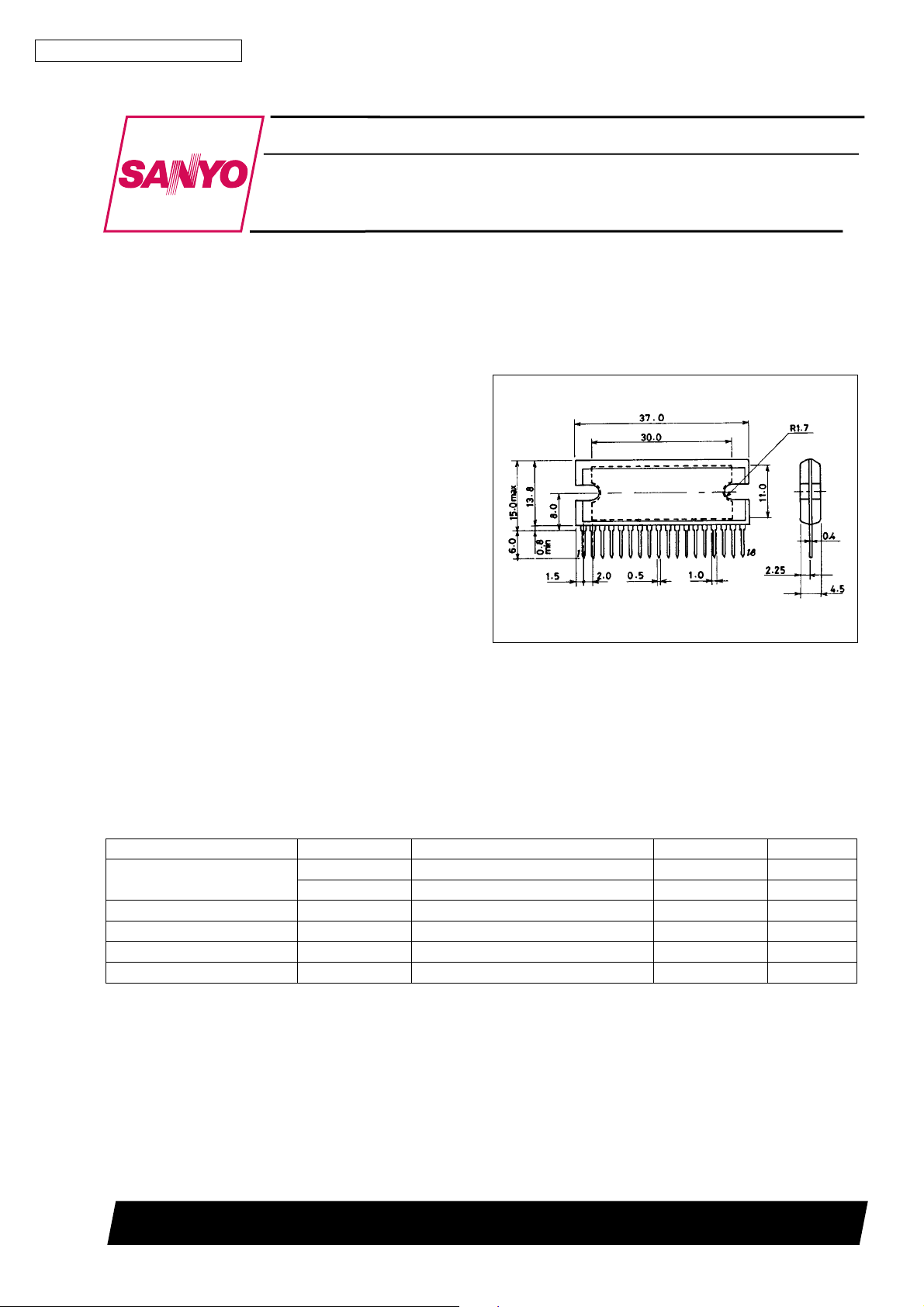
Package Dimensions
unit: mm
3109-SIP18H
[LA4705]
SANYO : SIP18H
Specifications
Maximum Ratings at Ta = 25°C
Parameter Symbol Conditions Ratings Unit
Maximum supply voltage V
Surge supply voltage V
Allowable power dissipation Pd max Arbitrarily large heat sink 37.5 W
Operating temperature Topr –35 to +85 °C
Storage temperature Tstg –40 to +150 °C
* Set VCC,RLin a range that does not exceed Pd max = 37.5 W
max 1 No signal,t=60s 24 V
CC
V
max 2 With signal 18 V
CC
surge t % 0.2 s, single giant pulse 50 V
CC
SANYO Electric Co.,Ltd. Semiconductor Bussiness Headquarters
TOKYO OFFICE Tokyo Bldg., 1-10, 1 Chome, Ueno, Taito-ku, TOKYO, 110 JAPAN
D3096HA(II)/12693TS/4152TS No.3848-1/8
LA4705
Operating Conditions at Ta = 25°C
Parameter Symbol Conditions Ratings Unit
Recommended supply voltage V
Operating voltage range V
Recommended load resistance R
CC
op Range where Pd max is not exceeded 9 to 18 V
CC
L
Operating Characteristics at Ta = 25°C, VCC= 13.2 V, RL=4Ω,f=1kHz, Rg = 600 Ω
Parameter Symbol Conditions min typ max Unit
Quiescent current I
Standby current Ist 10 60 µA
Voltage gain VG 38 40 42 dB
Total harmonic distortion THD P
Output power
Output offset voltage V
Output noise voltage V
Ripple rejection ratio SVRR Rg = 0, f
Channel separation CHsep Rg = 10 kΩ,V
Input resistance r
Standby pin applied voltage Vst Amp on, applied through 10 kΩ 2.5 V
CCO
= 1 W 0.1 0.4 %
1 THD = 10% 11 15 W
P
O
P
2 THD = 10%, VCC= 14.4 V 18 W
O
P
3 THD = 10%, RL=2Ω 16 W
O
offset Rg = 0 –300 +300 mV
N
NO
i
O
Rg = 0, B.P.F. = 20 Hz to 20 kHz 0.1 0.5 mVrms
= 100 Hz, VR= 0 dBm 40 50 dB
R
= 0 dBm 50 60 dB
O
13.2 V
4 Ω
80 115 250 mA
21 30 39 kΩ
CC
V
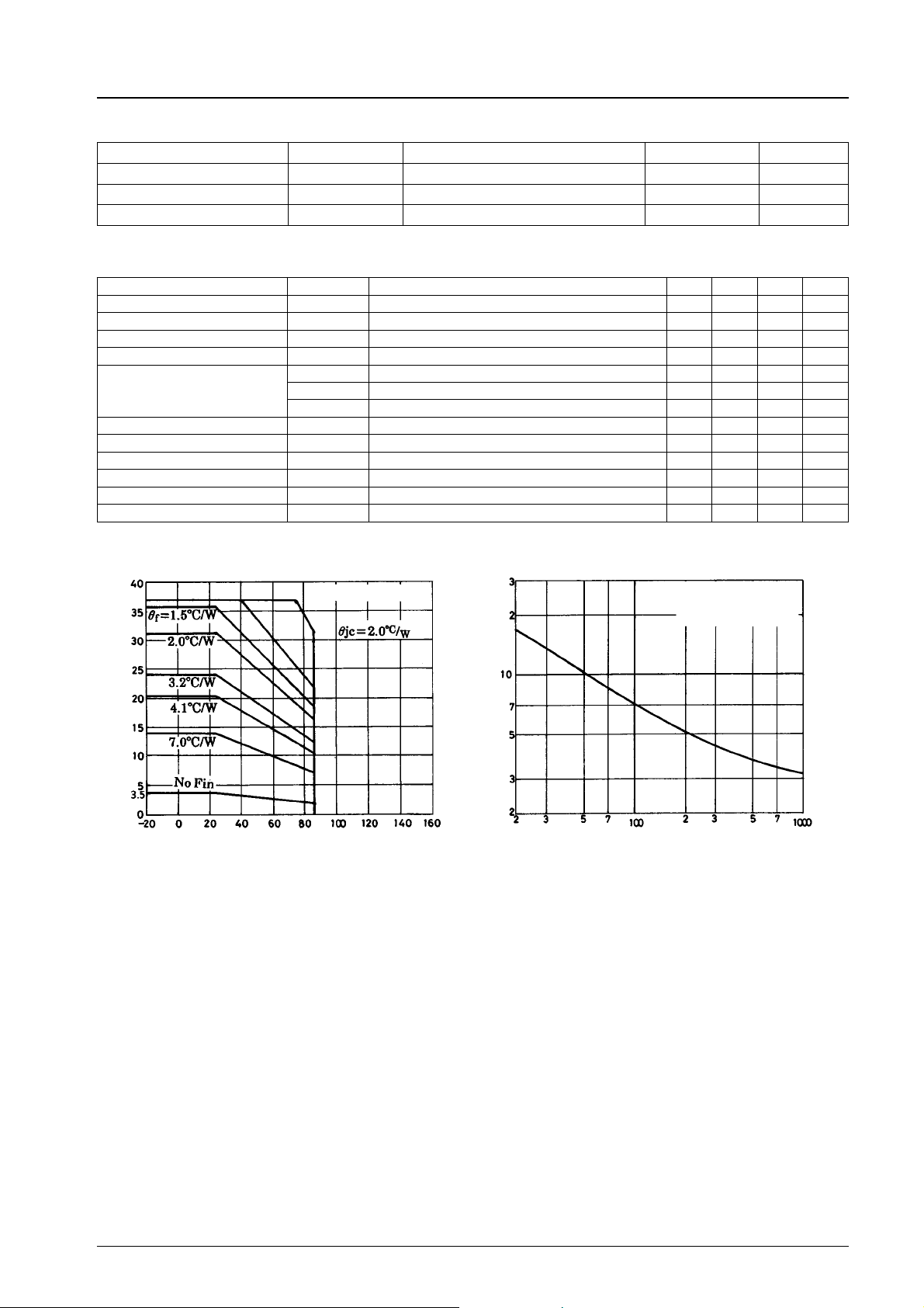
Allowable power dissipation, Pd max – W
Pd max – Ta
Arbitrarily large heat sink
Ambient temperature, Ta – °C
– °C/W
f
Heat sink thermal resistance, θ
θ
f–Sf
Al heat sink, t = 1.5 mm
Tightening torque 39 Nccm
With silicone grease applied
Heat sink area, Sf–cm
2
No.3848 -2/8
LA4705
Features and Usage Notes
.
Pin 5 is the standby switch pin. The amplifier is turned on by applying approximately 2 V or more to this pin through an
external resistor (R1). The current flowing into pin 5 is 500 µA or less.
.
Pin 6 is the mute pin. The amplifier on time can be set as desired through C3. By grounding pin 6, the amplifier can implement
mute operation. In this case, the recovery time depends on C3.
.
In order to prevent damage or degradation which may be caused by abnormally heated IC, the LA4705 has a thermal shutdown
protector. Accordingly, in the case of inadequate heat dissipation, the thermal shutdown protector will operate to control the
output gradually into attenuation.
.
Also be fully careful of handling other protectors built in the LA4705.
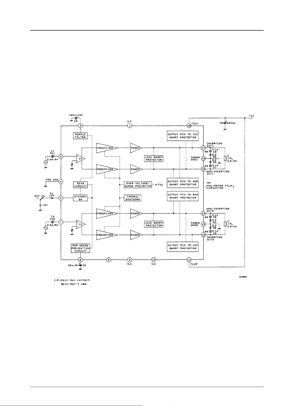
Sample Application Circuit
Unit (resistance: Ω, capacitance: F)
No.3848 -3/8
 Loading...