

Page 1
Any and all SANYO products described or contained herein do not have specifications that can handle
applications that require extremely high levels of reliability, such as life-support systems, aircraft’s
control systems, or other applications whose failure can be reasonably expected to result in serious
physical and/or material damage. Consult with your SANYO representative nearest you before using
any SANYO products described or contained herein in such applications.
SANYO assumes no responsibility for equipment failures that result from using products at values that
exceed, even momentarily, rated values (such as maximum ratings, operating condition ranges,or other
parameters) listed in products specifications of any and all SANYO products described or contained
herein.
Monolithic Linear IC
9V/12V 3-Dimension Power IC for
Radio Cassette Recorders
Ordering number:ENN3227A
LA4630N
SANYO Electric Co.,Ltd. Semiconductor Company
TOKYO OFFICE Tokyo Bldg., 1-10, 1 Chome, Ueno, Taito-ku, TOKYO, 110-8534 JAPAN
Features
• Stereo section 9V/3Ω 3W×2, 12V/3Ω 5W×2 : noise filter
capacitorless power.
• Super bus section 9V/3Ω 6W, 12V/3Ω 10W : output ca-
pacitor, B-S capacitorless power.
This chip employs technology for eliminating pins and
external connections to realize 3-dimensional power on a
single chip. This IC is a single package power IC for
making sound systems with punch.
• On-chip pop noise suppressor.
• On-chip power switch circuit.
• External and mute functions on chip.
• Protection functions on chip (thermal protection circuit
and BTL section RL short protection circuit)
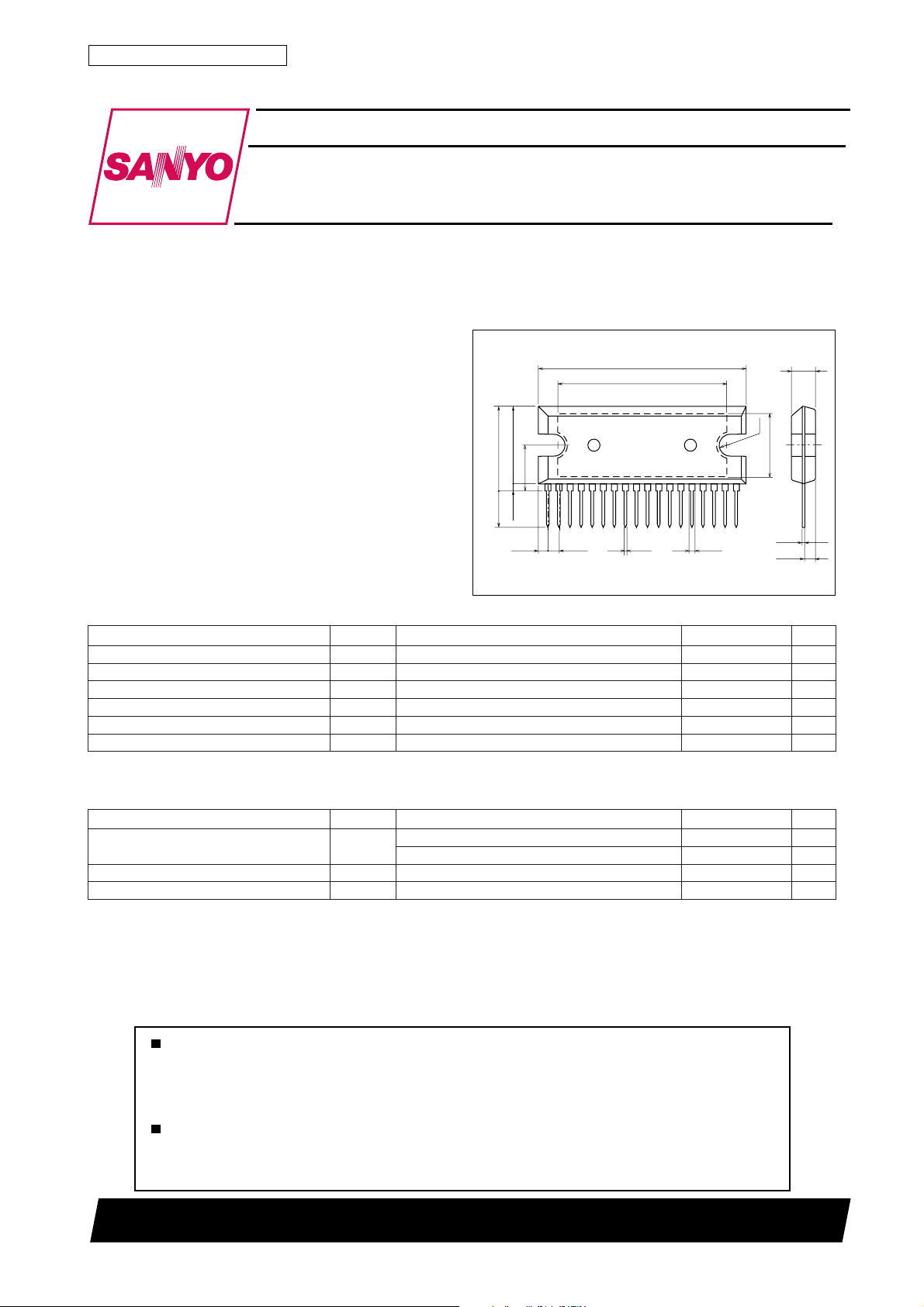
Package Dimensions
unit:mm
3109-SIP18H
[LA4630N]
37.0
30.0
13.8
15.0max
8.0
6.0
0.8min
1
1.5 2.0 1.0
0.5
4.5
R1.7
11.0
18
0.4
2.25
Specifications
SANYO : SIP18H
Maximum Ratings at Ta = 25˚C
retemaraPlobmySsnoitidnoCsgnitaRtinU
egatlovylppusmumixaMV
ecnatsiserlamrehT
tnerructuptuomumixaMI
noitapissidrewopelbawollAxamdPknistaehetinifnihtiW 5.73W
erutarepmetgnitarepOrpoT 57+ot02–
erutarepmetegarotSgtsT 051+ot04–
*1 : Operational notes on the maximum supply voltage.
xamlangison1* 02V
CC
θ c-j
kaep 3A
O
2
˚C/W
˚C
˚C
Recommended Operating Conditions at Ta = 25˚C
retemaraPlobmySsnoitidnoCsgnitaRtinU
egatlovylppusdednemmoceRV
ecnatsiserdaoldednemmoceRR
egatlovgnitarepOV
*2 : The upper limit for VCC op is VCC max – 2V. Continued on next page.
CC
L
po2* 81ot5V
CC
9V
21V
Ω
8ot3
40500TN (KT)/D191TH/5150TA, TS (GTPS) No.3227–1/8
Page 2
LA4630N
Continued from preceding page.
R/LTNORFLTBV
RL≥3Ω RL≥3Ω V02
RL≥3Ω RL≥4Ω V12
RL≥3Ω RL≥5Ω V22
RL≥3Ω RL≥6Ω V32
RL≥3Ω RL≥7Ω V42
RL≥3Ω RL≥8Ω V42
For power supply transistor regulation, the equivalent power line resistance is 3Ω or greater.
[Precaution concerning the metal]
Select PO with a goal of a rated load/rated supply voltage of RL=3 to 8Ω and VCC=5 to 18V and design to avoid
exceeding the package Pd max of 37.5W. For heavy loads or high VCC, the drive design is involved and the power
effect deteriotates, so pay attention to these factors.
Operating Characteristics at Ta = 25˚C, VCC=9V, RL=3Ω, f=1kHz
retemaraPlobmySsnoitidnoC
tnerrucni-wolftnecseiuQI
tnerrucybdnatSI
tnerrucni-wolfniphctiwsrewoPI
tnerrucni-wolfylppusetuMI
]noitceSoeretS[
rewoptuptuO
noitrotsidcinomrahlatoTDHTVOV1=02.00.1%
ecnatsisertupnIR
niagegatloVGV345474Bd
egatlovesiontuptuOV
noitcejerelppiRRVSfRV,zH001=
noitarapeslennahCpesHCk01=gR Ω V,
noitaunettagnituMA
ycneuqerfffollornoiger-woLf
ycneuqerfffollornoiger-hgiHf
]noitceSsuBrepuS[
rewoptuptuO
noitrotsidcinomrahlatoTDHTVOV1=02.00.1%
ecnatsisertupnIR
niagegatloVGV345474Bd
egatlovesiontuptuOV
noitcejerelppiRRVSfRV,zH001=
noitaunettagnituMA
ycneuqerfffollornoiger-woLf
ycneuqerfffollornoiger-hgiHf
egatlovtesffotuptuOV
xamsnoitidnoC
CC
OCC
TS
WS
m 0.530.07Am
CC
PO1V
PO2V
i
ON
tt
L
H
PO1V
PO2V
i
ON
tt
L
H
FFO
langisoN
0=gRroticapachtiwtupniR/LtnorF
0=gRroticapactuohtiwtupniR/LLTB
sgnitaR
nimpytxam
5307041Am
0.10.01Aµ
0.01Am
CC
CC
V
mBd0=08Bd
O
CC
CC
V
mBd0=08Bd
O
0=gR051–051+Vm
%01=DHT,V9=2.20.3W
%01=DHT,V21=2.40.5W
05kΩ
zHk02otzH02=FPB,0=gR51.004.0Vm
mBd0=5455Bd
R
mBd0=5405Bd
O
Bd3–=GVtA05zH
Bd3–=GVtA05zHk
%01=DHT,V9=0.50.6W
%01=DHT,V21=0.80.01W
03kΩ
zHk02otzH02=FPB,0=gR3.06.0Vm
mBd0=0506Bd
R
Bd3–:GV5zH
Bd3–:GV04zHk
tinU
No.3227–2/8
Page 3
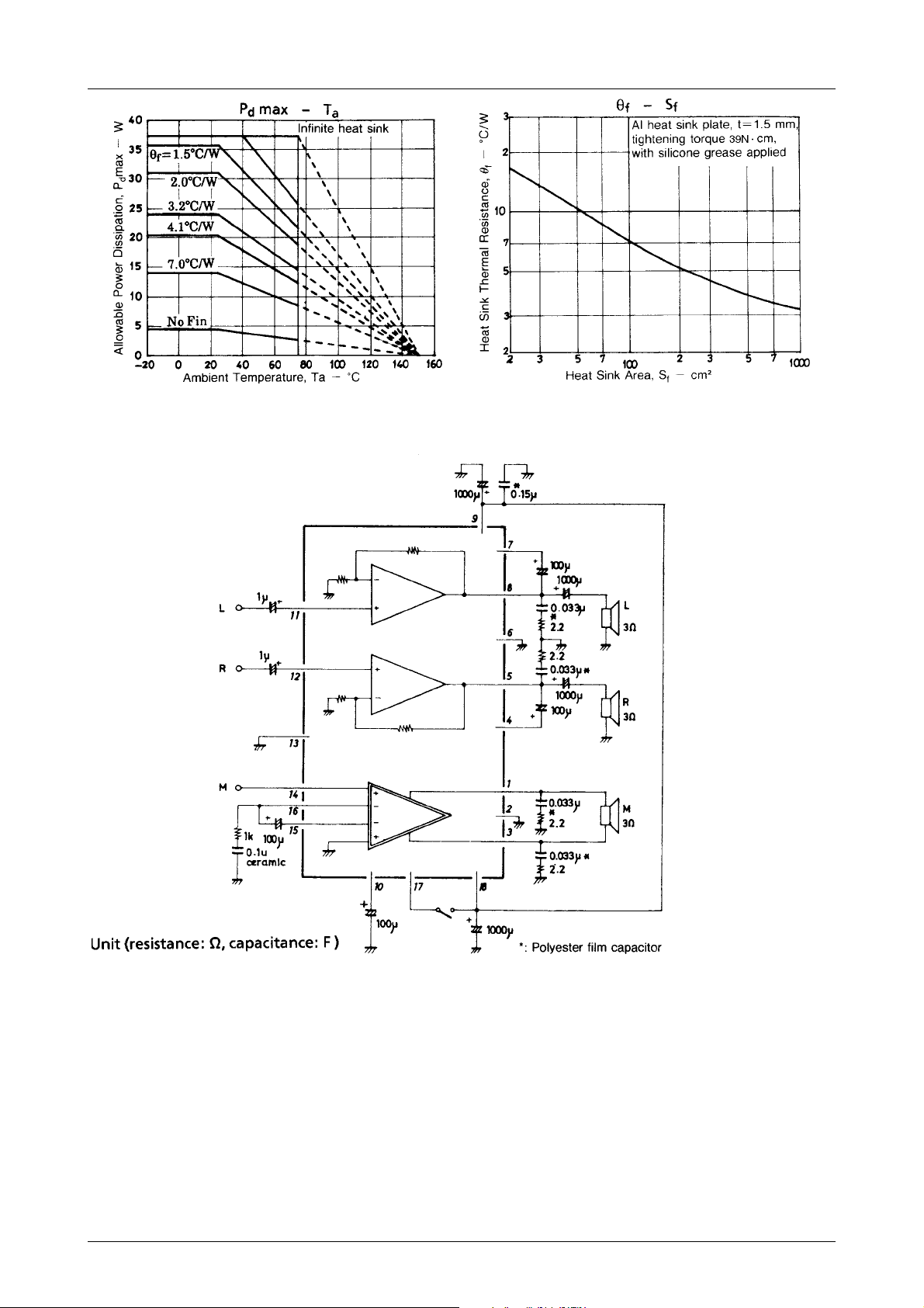
Block Diagram
LA4630N
Note 1 : The motor should not be connected to the power switch pin, since transient noise may appear on the amplifier
outputs when the motor is started or stopped.
Note 2 : Audio mute is enabled by connecting a 300Ω resistance between the DC pin and ground. DC bias control of
both the stereo (L ch, R ch) and BTL (super bass) channels is enabled, and all audio output signals can be
muted by controlling the MUTE pin.
No.3227–3/8
Page 4

Sample Printed Circuit Pattern
LA4630N
* : Insert 0.15µF between power supply and ground at the root of the pins.
Pin Voltages
.oNniP 123456789
TUO
RWP
TUO
emaN
)V(
.oNniP011121314151617181
emaNCD
)V(
oN
egatloVniP
0.400.41.85.401.80.40.9
egatloVniP
5.44.14.10
DNG
2
NI
NI
L
R
SB
vnI
R
TUO
R
ERP
NI
DNG
oN
12
]Vm[
PO Chart (THD=10%) Pd max Chart
metIRLV9V21V51
8Ω W4.1W5.2W9.3
TNORF
R/L
LTB
6Ω W57.1W2.3W0.5
4Ω W4.2W3.4W4.6
3Ω W2.3W6.5–
8Ω W2.3W4.6W0.11
6Ω W0.4W1.8W5.31
4Ω W3.5W4.01–
3Ω W4.6W4.21–
metIRLV9V21V51
TNORF
R/L
LTB
RWP
SB
DNG
L
1
FN
FN
vnI
oN
4.14.10.90.9
8Ω W0.2W2.3W6.4
6Ω W4.2W8.3W7.5
4Ω W1.3W0.5W4.5
3Ω W8.3W2.6–
8Ω W8.2W8.4W2.7
6Ω W6.3W0.6W0.9
4Ω W0.5W8.8–
3Ω W3.6W2.11–
TUO
V
L
WS
CC
1
RWP
V
CC
2
No.3227–4/8
Page 5

LA4630N
No.3227–5/8
Page 6

LA4630N
No.3227–6/8
Page 7

LA4630N
Notes on using this IC
• Alw ays shor t power supply pins 9 and 16 on the copper foil of the printed circuit pattern and apply the equivalent po wer
supply voltage.
• Pin 17 is designed for the power switch.
It can be switched on and off with a small current capacitance switch, but the point to watch out for is tha t if the voltgae
loss between pins 17 and 18 is too large, there may be problems in the biasing and the power may drop.
• When switching with a transistor, the general practice is to insert a PNP transistor between pins 17 and 18.
Notes on Mounting Radiator Fin
1. The tightening torque should be in the range of 39 to 59N · cm.
2. The distance between screw holes of the radiator fin must coincide with the distance between screw holes of the IC.
With case outline dimensions L and R referred to the screws must be tightened with the distance between them as
close to each other as possible.
3. The screw to be used must ha v e a head equivalent to the one of truss machine screw or binder machine screw defined
by JIS. Washers must be also used to protect the IC case.
4. No foreign matter such as cutting particles shall exist between heat sink and radiator fin. When applying grease on the
junction surface, it must be applied uniformly on the whole surface.
5. IC lead pins are soldered to the printed circuit board after the radiator fin is mounted on the IC.
No.3227–7/8
Page 8

LA4630N
Specifications of any and all SANYO products described or contained herein stipulate the performance,
characteristics, and functions of the described products in the independent state, and are not guarantees
of the performance, characteristics, and functions of the described products as mounted in the customer's
products or equipment. To verify symptoms and states that cannot be evaluated in an independent device,
the customer should always evaluate and test devices mounted in the customer's products or equipment.
SANYO Electric Co., Ltd. strives to supply high-quality high-reliability products. However, any and all
semiconductor products fail with some probability. It is possible that these probabilistic failures could
give rise to accidents or events that could endanger human lives, that could give rise to smoke or fire,
or that could cause damage to other property. When designing equipment, adopt safety measures so
that these kinds of accidents or events cannot occur. Such measures include but are not limited to protective
circuits and error prevention circuits for safe design, redundant design, and structural design.
In the event that any or all SANYO products(including technical data,services) described or
contained herein are controlled under any of applicable local export control laws and regulations,
such products must not be exported without obtaining the export license from the authorities
concerned in accordance with the above law.
No part of this publication may be reproduced or transmitted in any form or by any means, electronic or
mechanical, including photocopying and recording, or any information storage or retrieval system,
or otherwise, without the prior written permission of SANYO Electric Co. , Ltd.
Any and all information described or contained herein are subject to change without notice due to
product/technology improvement, etc. When designing equipment, refer to the "Delivery Specification"
for the SANYO product that you intend to use.
Information (including circuit diagrams and circuit parameters) herein is for example only ; it is not
guaranteed for volume production. SANYO believes information herein is accurate and reliable, but
no guarantees are made or implied regarding its use or any infringements of intellectual property rights
or other rights of third parties.
This catalog provides information as of April, 2000. Specifications and information herein are subject to
change without notice.
PS No.3227–8/8
 Loading...