

SANYO LA4625 Datasheet
Ordering number : ENN6631
92900RM (OT) No. 6631-1/8
Overview
The LA4625 is a 2-channel general-purpose BTL audio
power amplifier provided in a miniature package. It was
designed for the best possible audio quality and features
an extended low band roll-off frequency provided by a
newly-developed NF circuit that does not require an
external capacitor. Furthermore, crosstalk, which can
cause muddiness in the audio output, has been
significantly reduced by both circuit and wiring pattern
improvements. Thus this amplifier can provide powerful
lows and clear highs.
Note that this device is pin compatible with the 20 W × 2-
channel LA4628, and allows end products differentiated
by their power rating to share the same printed circuit
board.
Features
• Total output: 13.5 W + 13.5 W (at VCC= 12 V, RL = 4 Ω,
THD = 10%)
• PMPO reference data: 115 W × 2 (VCC= 20 V, RL = 4 Ω)
• High-fidelity design (fL< 10 Hz, fH= 130 kHz)
• Extremely low impulse noise levels
• An arbitrary amplifier startup time can be set up with
external components.
• Full complement of built-in protection circuits (includes
circuits that protect against shorting to VCC, shorting to
ground, load shorting, overvoltages and excessive
temperatures)
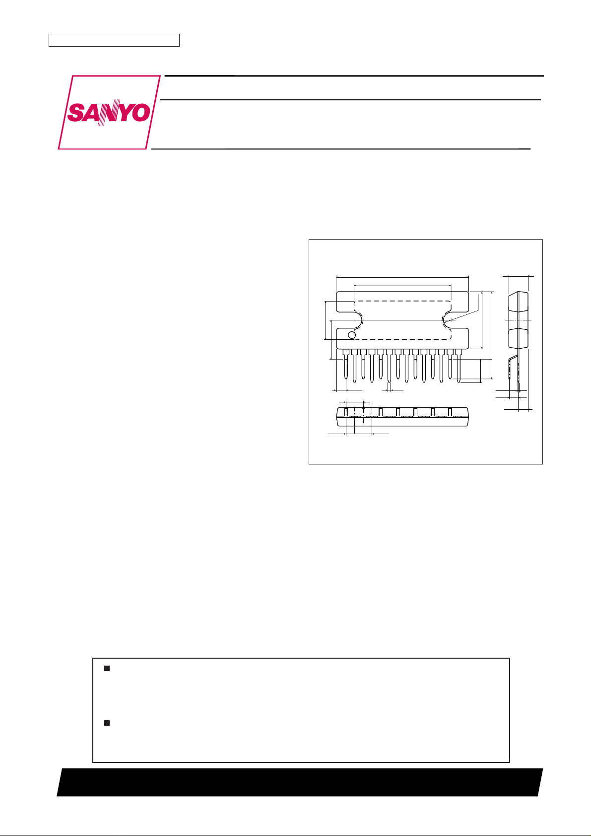
Package Dimensions
unit: mm
3113A-SIP14HZ
27.0
20.0
R1.7
0.5
1.94
8.4
7.8
14.5max
14
1
0.4
11.8
5.2
4.6
1.6
2.2
4.0
1.78 3.56
3.56
SANYO: SIP14HZ
[LA4625]
LA4625
SANYO Electric Co.,Ltd. Semiconductor Company
TOKYO OFFICE Tokyo Bldg., 1-10, 1 Chome, Ueno, Taito-ku, TOKYO, 110-8534 JAPAN
Two-Channel 13.5 W BTL Audio Power Amplifier
Monolithic Linear IC
Any and all SANYO products described or contained herein do not have specifications that can handle
applications that require extremely high levels of reliability, such as life-support systems, aircraft’s
control systems, or other applications whose failure can be reasonably expected to result in serious
physical and/or material damage. Consult with your SANYO representative nearest you before using
any SANYO products described or contained herein in such applications.
SANYO assumes no responsibility for equipment failures that result from using products at values that
exceed, even momentarily, rated values (such as maximum ratings, operating condition ranges, or other
parameters) listed in products specifications of any and all SANYO products described or contained
herein.
No. 6631-2/8
LA4625
Parameter Symbol Conditions Ratings Unit
Maximum supply voltage V
CC
max No signal 24 V
Maximum output current I
O
peak Per channel 3.5 A
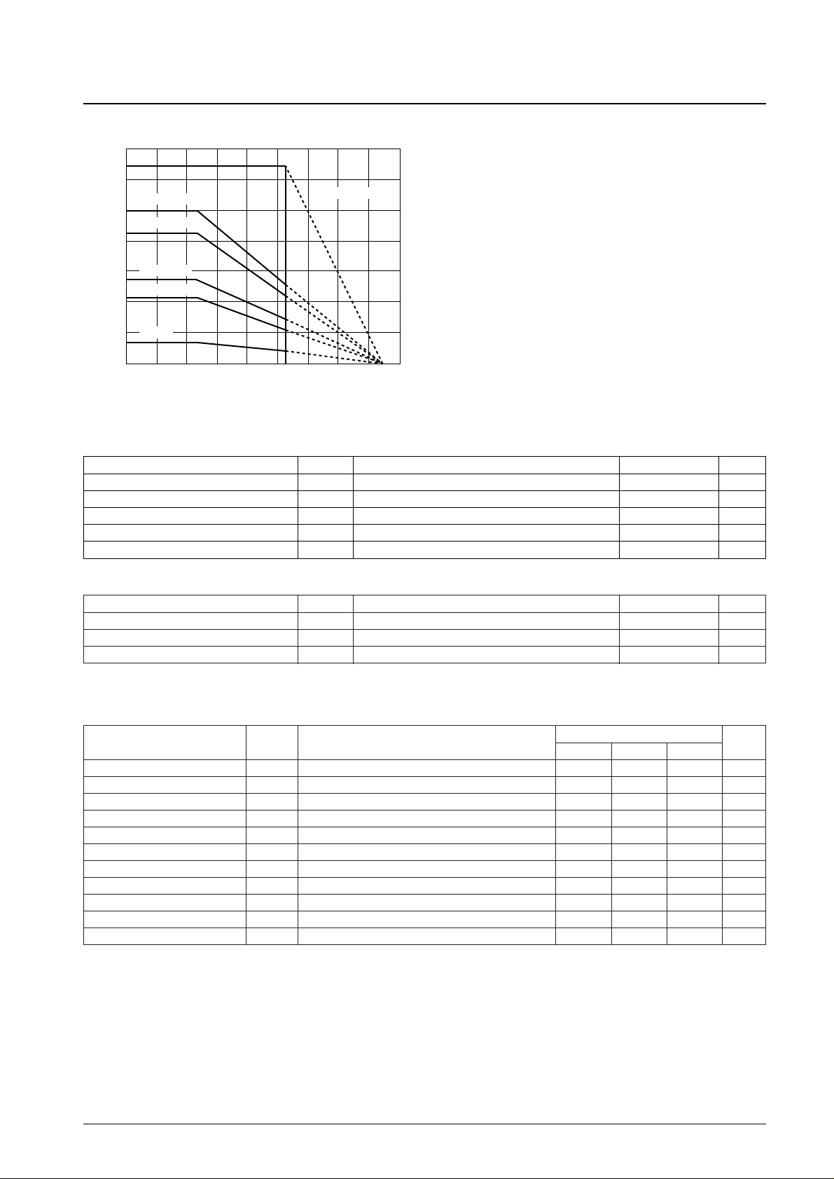
Allowable power dissipation Pd max With an arbitrarily large heat sink 32.5 W
Operating temperature Topr –20 to +85 °C
Storage temperature Tstg –40 to +150 °C
Specifications
Maximum Ratings at Ta = 25°C
Parameter Symbol Conditions Ratings Unit
Recommended supply voltage V
CC
12 V
Recommended load resistance range RL op 4 to 8 Ω
Allowable operating supply voltage range V
CC
op 7.2 to 20 V
Operating Conditions at Ta = 25°C
Note: With VCC, RL, and the output level in ranges such that the Pdmax for the heat sink used is not exceeded.
Pd max — Ta
Ambient temperature, Ta —°C
10
15
0
–20 0 20 40 1601401201008060
5
20
25
30
35
Allowable power dissipation, Pd max — W
θjc=2.0°C/W
θf=3°C/W
θf=4°C/W
θf=7°C/W
θf=10°C/W
No Fin
Parameter Symbol Conditions
Ratings
Unit
min typ max
Quiescent current I
CCO
Rg = 0 65 120 240 mA
Standby mode current drain I
st
Standby mode (amplifier off), with no power supply capacitor.
10 60 µA
Voltage gain V
G
VO= 0 dBm 38 40 42 dB
Total harmonic distortion THD P
O
= 1 W, Filter = FLAT 0.06 0.2 %
Output power P
O
1 THD = 10% 10 13.5 W
Output offset voltage V
N
offset Rg = 0 –300 +300 mV
Output noise voltage V
NO
Rg = 0, BPF = 20 Hz to 20 kHz 0.1 0.5 mV
Ripple rejection ratio SVRR Rg = 0, VR = 0 dBm, fR = 100 Hz 40 50 dB
Channel separation CH Sep Rg = 10 kΩ, V
O
= 0 dBm 50 60 dB
Input resistance Ri 21 30 39 kΩ
Standby pin applied voltage V
ST
Amplifier on (applied through an external 10 kΩ resistor) 2.5 V
CC
V
Operating Characteristics at Ta = 25°C, VCC= 12 V, RL = 4 Ω, f = 1 kHz, Rg = 600 Ω
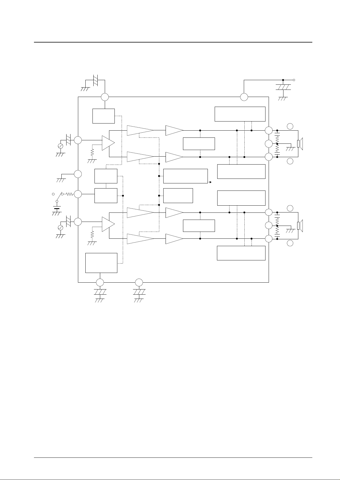
Equivalent Circuit Block Diagram
No. 6631-3/8
LA4625
C8 0.1 µ
R4
2.2
C9 0.1 µ
R5
2.2
RL
4 Ω
–OUT2
+OUT2
–
+
Standby
SW
OFF
RIPPLE
FILTER
+
BIAS
CIRCUIT
STANDBY
SW
POP NOISE
PREVENTION
CIRCUIT
PREDRIVER
PREDRIVER
POWER
POWER
LOAD SHORT
PROTECTOR
OUTPUT PIN TO V
CC
SHORT PROTECTOR
OUTPUT PIN TO V
CC
SHORT PROTECTOR
OUTPUT PIN TO GND
SHORT PROTECTOR
OUTPUT PIN TO GND
SHORT PROTECTOR
PREDRIVER
PREDRIVER
POWER
POWER
OVER VOLTAGE/
SURGE
THERMAL
SHUT DOWN
LOAD SHORT
PROTECTOR
V
CC
+
+
ON
R1
10 K
+5 V
C4
2.2 µ
10 V
33 µ
10 V
0.47 µ
10 V
2.2 µ
10 V
C1
100 µ/16 V
V
CC
C5
2200 µ
25 V
+
**
**
C6 0.1 µ
R2
2.2
C7 0.1 µ
R3
2.2
RL
4 Ω
–OUT1
+OUT1
–
+
**
**
POWER
GND2
+ +
C3
C10
**
(POLYESTER
FILM
CAPACITOR)
+
–
IN
+
–
IN
C2
PRE GND
IN2
C3 C10
Sets the amplifier starting time
(Approximately 0.6 seconds when 33 µF)
Impulse noise reduction
(Note: The device’s ability to withstand shorting
to V
CC
or shorting to ground when VCC is around
16 V may be reduced as the value of this
capacitor is increased. We recommend 0.47 µF.)
POWER
GND1
14
2
1
3
4
6
7
5
8
10
9
11
12
13
 Loading...