

Page 1
Ordering number: EN3535A
Monolithic Linear IC
LA4581MB
Preamplifier + Power Amplifier
for 3V Headphone Stereos
Overview
The LA4581MB is an auto reverse-supported preamplifier +
power amplifier IC that is intended for use in 3V headphone
stereos.
Features
.
Preamplifier muting and preamplifier output on/off can be
implemented with one pin. This IC can easily be used to
construct a set with a radio.
.
The power amplifier needs no input/output coupling
capacitor.
.
A high-frequency cut capacitor is connected to the
preamplifier input pin and the power amplifier input pin.
(Anti-buzz provision)
.
Because V
grounding impedance is about 10 Ω. This eliminates the
need for a large capacitor.
.
8 Ω speaker drivable.
AMP (r0=10Ω) is built in, the virtual
ref
Specifications
Maximum Ratings atTa=25°C
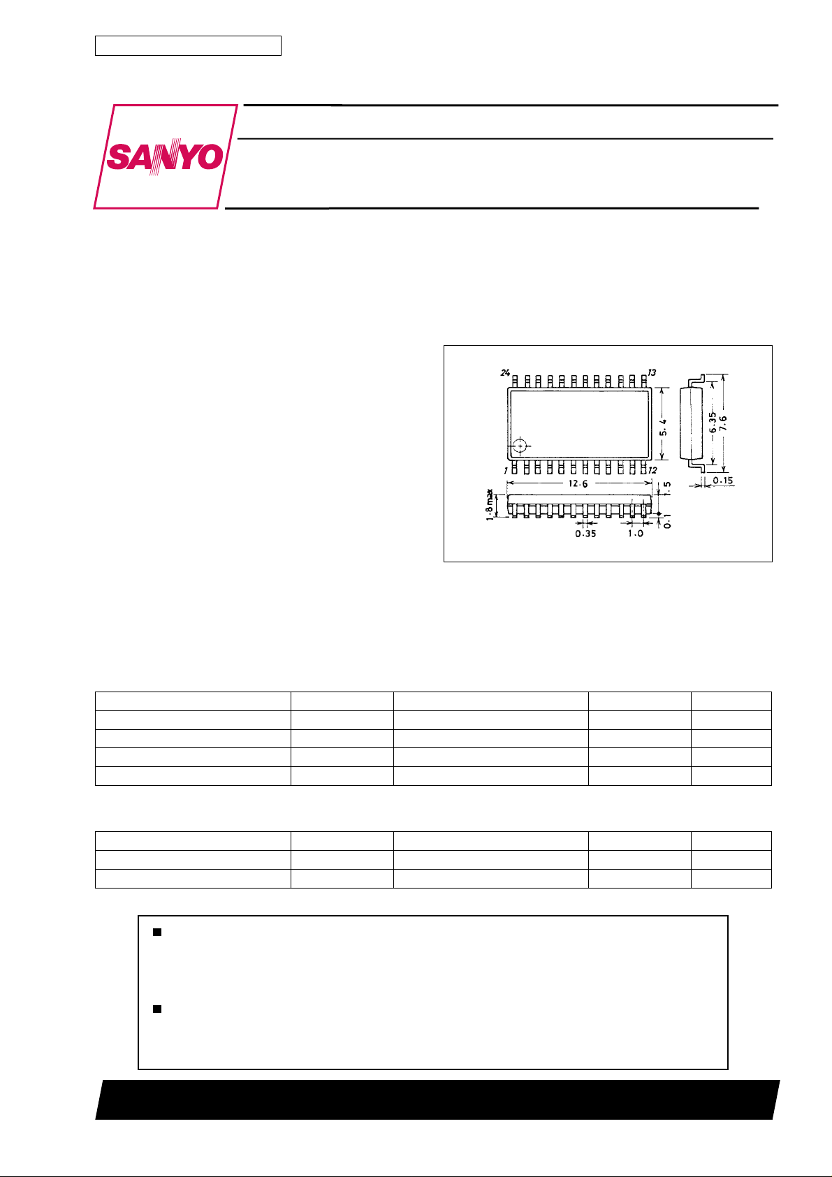
Package Dimensions
unit : mm
3112-MFP24S
[LA4581MB]
SANYO : MFP24S
Parameter Symbol Conditions Ratings Unit
Maximum supply voltage V
Allowable power dissipation Pd max 530 mW
Operating temperature Topr –20 to +75
Storage temperature Tstg –40 to +125
max 4.5 V
CC
Operating Conditions atTa=25°C
Parameter Symbol Conditions Ratings Unit
Recommended supply voltage V
Operating supply voltage range V
Any and all SANYO products described or contained herein do not have specifications that can handle
applications that require extremely high levels of reliability, such as life-support systems, aircraft’s
control systems, or other applications whose failure can be reasonably expected to result in serious
physical and/or material damage. Consult with your SANYO representative nearest you before using
any SANYO products described or contained herein in such applications.
SANYO assumes no responsibility for equipment failures that result from using products at values that
exceed, even momentarily, rated values (such as maximum ratings, operating condition ranges, or other
parameters) listed in products specifications of any and all SANYO products described or contained
herein.
CC
op 1.8 to 3.6 V
CC
3.0 V
SANYO Electric Co.,Ltd. Semiconductor Bussiness Headquarters
TOKYO OFFICE Tokyo Bldg., 1-10, 1 Chome, Ueno, Taito-ku, TOKYO, 110-8534 JAPAN
22896HA(II) No.3535-1/10
C
°
C
°
Page 2
LA4581MB
Operating Characteristics atTa=25°C, VCC=3.0V,f=1kHz, 0.775 V = 0 dBm,
=10kΩ(preamplifier), RL=16Ω(power amplifier)
R
L
Parameter Symbol
Output
min typ max Unit
[Pre + Power]
Quiescent current I
CCO
Voltage gain (Closed) VG
Rg = 2.2 kΩ (preamplifer) VIN= 0 V 17 27 mA
VO= –5 dBm 65 68 71 dB
T
[Preamplifier]
Voltage gain (Open) VGo V
Voltage gain (Closed) VG1 V
Maximum output voltage V
max THD=1%,VCC= 1.8 V 0.1 0.2 V
O
Total harmonic distortion THD1 V
Equivalent input noise voltage V
1 Rg = 2.2 kΩ, B.P.F = 20 to 20 kHz 1.3 2.0 µV
N
= –5 dBm 70 80 dB
O
= –5 dBm 40 dB
O
= 0.2 V, VG = 40 dB/NAB 0.05 0.5 %
O
Crosstalk CT1 Rg = 2.2 kΩ, TUNE 1 kHz 60 80 dB
Ripple rejection ratio R
1
r
Rg = 2.2 kΩ,V
f = 100 Hz
= 1.8 V, Vr = –20 dBm,
CC
40 50 dB
[Power Amplifer]
Output voltage P
Voltage gain (Closed) VG2 V
Total harmonic distortion THD2 P
Interchannel crosstalk CT
Output noise voltage V
NO
Ripple rejection ratio R
Input resistance R
DC offset voltage V
ODC
THD = 10% 23 32 mW
O
T
= –5 dBm 25 28 31 dB
O
= 1 mW 0.4 1.0 %
O
VO= –5 dBm, Rv=0Ω 30 40 dB
Rg = 0, B.P.F = 20 to 20 kHz 24 40 µV
2 Rg=0,Vr= –20 dB, f = 100 Hz, VCC= 1.8 V 45 60 dB
r
IN
22 30 38 kΩ
off Between 13-14 and 15 –90 +90 mV
Note) Power amplifier voltage gain VG2 increases by about 1 dB for min/max respectively than specified above when RL=32Ω.
No.3535-2/10
Page 3
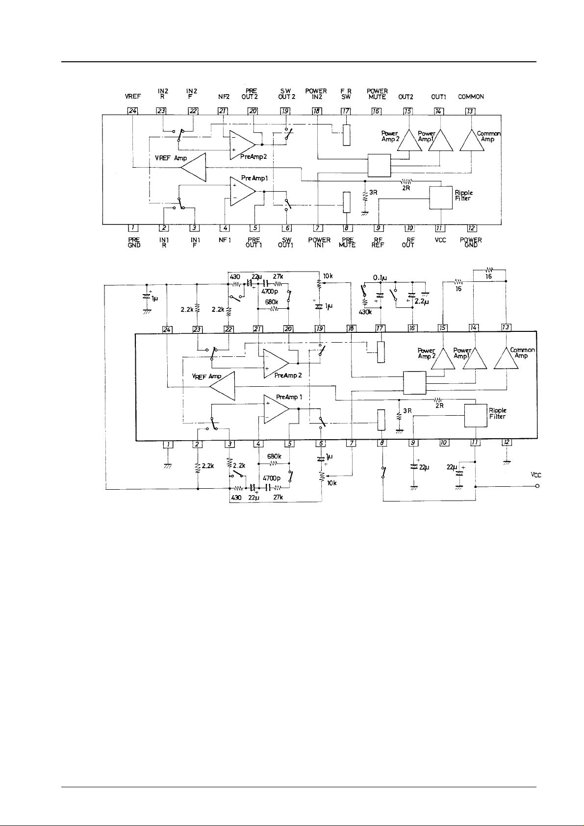
Block Diagram
Test Circuit
LA4581MB
1.8 to 3.0 V
Unit (resistance: Ω, capacitance: F)
No.3535-3/10
Page 4

LA4581MB
Allowable power dissipation, Pd max – mW
Ambient temperature, Ta –°C
Sample Application Circuit
Note) Pre closed loop gain VG = 40 dB/1 kHz NAB
Preamplifier input is applied to pins 2,23/
pins 3,22 when SW ON/OFF, respectively.
PRE MUTE ON when
connected to V
POWER MUTE ON when
connected to GND.
1.8 to 3.6 V
CC
Unit (resistance: Ω, capacitance: F)
Pin and external part functions (when the voltage is V
Pin No. Pin Function
1 PRE GND
PRE IN1R 1.8 V
2
v Turns ON when pin 17 is grounded.
v A bias resistor (2.2 kΩ) must be connected between pin 2 and pin 24 (V
PRE IN1F 1.8 V
3
v Turns ON when pin 17 is floating.
v A bias resistor (2.2 kΩ) must be connected between pin 3 and pin 24 (V
4 PRE NF1 1.8 V
PRE OUT1 1.8 V
5
v Like pin 6, 10 kΩ load drivable.
SW OUT1 1.8V
6
v Provides PRE AMP1 output when pin 8 is floating (PRE MUTE OFF)(equivalent to pin 5).
v Disconnects from PRE AMP1 and sets R
POWER IN1 1.8V
7
v Input resistance R
7 30 kΩ
IN
^ 500 kΩ when pin 8 is at VCC(PRE MUTE ON).
IN
= 3.0 V)
CC
) when no head is in use.
ref
) when no head is in use.
ref
Continued on next page.
No.3535-4/10
Page 5

LA4581MB
Continued from preceding page.
Pin No. Pin Function
PRE MUTE
8
v When V
v MUTE ON conditions: V
Ripple Filter REF 2.7 V(C
v Ripple Filter, V
9
v The V
v R
is 55 dB for 22 µF; 35 dB for 2.2 µF.
r
Ripple Filter OUT 2.7 V
10
v Ripple rejection ratio: R
v Outflow current I
11 V
CC
12 POWER GND
13 COMMON 1.2 V
POWER OUT1 1.2 V
14
v CH1 output.
POWER OUT2 1.2 V
15
v CH2 output
POWER MUTE 0.7 V (C
v When connected to GND: POWER MUTE ON.
16
v MUTE ON conditions: V
v C
10
v When C
FWD/REV SW (C11 % 0.47 µF)
v When connected to GND, PRE IN1R (pin 2) and IN2R (pin 23) turn on.
17
v When floating, PRE IN1F (pin 3) and IN2F (pin 22) turn on.
v C
11
v REV condition: V
POWER IN2 1.8 V
18
v Input resistance R
SW OUT2 1.8 V
19
v Provides PRE AMP2 when pin 8 is floating (PRE MUTE OFF) (equivalent to pin 20).
v Disconnects from PRE AMP2 and R
PRE OUT2 1.8 V
20
v Like pin 19, 10 kΩ load drivable.
21 PRE NF2 1.8V
PRE IN2F 1.8 V
22
v Turns on when pin 17 is floating.
v A bias resistor (2.2 kΩ) must be connected between pin 22 and pin 24 (V
PRE IN2R 1.8 V
23
v Turns on when pin 17 is connected to GND.
v A bias resistor (2.2 kΩ) must be connected between pin 23 and pin 24(V
V
1.8 V
24
ref
v The reference voltage is set to 3/5 × V
v Inflow/outflow current I
is applied, PRE MUTE ON.
CC
reference
ref
ripple rejection ratio worsens when C7is made smaller.
ref
max=1mA
7
^ VCC– 0.2 V, inflow current I77 60 µA (when VCC=3V)
8IN
= 2.2 µF to 33 µF)
7
is 38 dB when C7= 22 µF; 30 dB when C7= 2.2 µF.
r
3.0 V
= 1.0 µF to 4.7 µF)
10
% 0.3 V, outflow current I167 2.5 µA.
can be used to control MUTE TIME.
= 2.2 µF, VCC=3.0 V 0.7 sec.
10
16
and R7are intended for smoothing at the time of switching.
% 0.2 V.
17
7 30 kΩ
IN
^ 500 kΩ when pin 8 is VCC(PRE MUTE ON).
IN
. Because Vref AMP (rO7 10 Ω) is built in, C17can be made smaller (1 µF).
= ± 500 µA available.
24
CC
) when no head is in use.
ref
) when no head is in use.
ref
Sample Application:
Radio set application.
As shown above, Radio on and
Pre Mute can be implemented with one-circuit
switch.
No.3535-5/10
Page 6

LA4581MB
IC Usage Notes
1. The power amplifier outputs and the common amplifier output are connected through resistors of about 60 Ω. The resistors
are for common amplifier oscillation blocking.
Ω
2. The preamplifier muting function isolates the preamplifier outputs from SW OUT. The preamplifier is on even when the
preamplifier muting is on.
3. If transient noise is noticeable when the power supply is turned off, add the external circuit described below. Transient noise
when the power is turned off can be improved by rapidly applying the power amplifier muting.
Unit (resistance: Ω, capacitance: F)
4. Internal equivalent circuit for each SW pin.
.
Pre-mute
Ω
However, the standby current ISTflows even when the
power switch is off
I
=(VCC–VBE)/600 kΩ
ST
When V
I
ST
= 3.0 V
CC
= (3.0 – 0.6)/600 kΩ 7 4µA
.
Power mute
.
F/R SW
Unit (resistance: Ω)
Unit (resistance: Ω, capacitance: F)
MUTE ON condition : V
Inflow current : I
MUTE ON condition : V16% 0.3 V
Outflow current : I
REV condition : V17% 0.2 V
7 60 µA (when VCC= 3.0 V)
8
16
^ VCC– 0.2 V
8IN
7 2.5 µA
Unit (resistance: Ω, capacitance: F)
No.3535-6/10
Page 7

LA4581MB
Quiescent current, Icco – mA
Pre + Power
Preamp
Supply voltage, VCC–V
Preamp
Voltage gain, VG – dB
Unit (resistance: Ω, capacitance: F)
Frequency,f–Hz
Preamp
Voltage gain, VGo – dB
Preamp
max–V
o
Maximum output voltage, V
[Between F/R]
Supply voltage, VCC–V
The base correction turns off, causing output
DC to increase, and output is obtained.
Supply voltage, VCC–V
89 dB at tune 1 kHz
Total harmonic distortion, THD – %
Output voltage, Vo–V
[Interchannel]
Preamp
79 dB at tune 1 kHz
Crosstalk, CT – dB
Frequency,f–Hz
Preamp
–µF
NO
equivalent
equivalent
Preamp
Crosstalk, CT – dB
Output noise voltage, V
ch1, ch2 equivalent
Frequency,f–Hz
Supply voltage, VCC–V
No.3535-7/10
Page 8

LA4581MB
amp
– dBm
o
Unit (resistance: Ω, capacitance: F)
Output voltage, V
Frequency,f–Hz
–V
DC
DC voltage, V
Drops because of 1 µF at
5 kH or more when
impedance is small.
Reference voltage, Vref – V
–V
DC
DC voltage, V
Virtual grounding inflow current is I = 500 µA max.
Output current, Io–mA
Power amp
(Vitrual
Grounding)
amp
–V
O
Maximum output voltage, V
Power amp
Supply voltage, V
Power amp
Supply voltage, VCC–V
When both channels output simultaneously
–V
CC
Supply voltage, VCC–V
Power amp
Voltage gain, VG – dB
When both channels output simultaneously
Frequency,f–Hz
Voltage gain, VG – dB
Crosstalk, CT – dB
When both channels output
Supply voltage, VCC–V
Frequency,f–Hz
Power amp
equivalent
No.3535-8/10
Page 9

LA4581MB
Total harmonic distortion,THD – %
Power amp
Power amp
When both channels output simultaneously
Supply voltage, VCC–V
Total harmonic distortion, THD – %
–µV
NO
Power amp
When both channels output simultaneously
Output voltage, P
–mW
O
Power amp
Total harmonic distortion, THD – %
When both channels output simultaneously
Output power, PO–mW
Output noise voltage, V
Supply voltage, V
CC
–V
Preamp
CC
–V
Power amp
SVRR – dB
ch1 and ch2 OUT are equivalent
Supply voltage, V
CC
–V
SVRR – dB
Supply voltage, V
No.3535-9/10
Page 10

LA4581MB
Specifications of any and all SANYO products described or contained herein stipulate the performance,
characteristics, and functions of the described products in the independent state, and are not guarantees
of the performance, characteristics, and functions of the described products as mounted in the customer’s
products or equipment. To verify symptoms and states that cannot be evaluated in an independent device,
the customer should always evaluate and test devices mounted in the customer’s products or equipment.
SANYO Electric Co., Ltd. strives to supply high-quality high-reliability products. However, any and all
semiconductor products fail with some probability. It is possible that these probabilistic failures could
give rise to accidents or events that could endanger human lives, that could give rise to smoke or fire,
or that could cause damage to other property. When designing equipment, adopt safety measures so
that these kinds of accidents or events cannot occur. Such measures include but are not limited to protective
circuits and error prevention circuits for safe design, redundant design, and structural design.
In the event that any or all SANYO products(including technical data,services) described or
contained herein are controlled under any of applicable local export control laws and regulations,
such products must not be exported without obtaining the export license from the authorities
concerned in accordance with the above law.
No part of this publication may be reproduced or transmitted in any form or by any means, electronic or
mechanical, including photocopying and recording, or any information storage or retrieval system,
or otherwise, without the prior written permission of SANYO Electric Co. , Ltd.
Any and all information described or contained herein are subject to change without notice due to
product/technology improvement, etc. When designing equipment, refer to the “Delivery Specification”
for the SANYO product that you intend to use.
Information (including circuit diagrams and circuit parameters) herein is for example only ; it is not
guaranteed for volume production. SANYO believes information herein is accurate and reliable, but
no guarantees are made or implied regarding its use or any infringements of intellectual property rights
or other rights of third parties.
This catalog provides information as of February, 1996. Specifications and information herein are subject to
change without notice.
PS No.3535-10/10
 Loading...