

Page 1
Any and all SANYO products described or contained herein do not have specifications that can handle
applications that require extremely high levels of reliability, such as life-support systems, aircraft’s
control systems, or other applications whose failure can be reasonably expected to result in serious
physical and/or material damage. Consult with your SANYO representative nearest you before using
any SANYO products described or contained herein in such applications.
SANYO assumes no responsibility for equipment failures that result from using products at values that
exceed, even momentarily, rated values (such as maximum ratings, operating condition ranges,or other
parameters) listed in products specifications of any and all SANYO products described or contained
herein.
Monolithic Linear IC
Low-voltage Headphone Amplifier
for Stereo Audio
Ordering number:ENN3534
LA4571MB
SANYO Electric Co.,Ltd. Semiconductor Company
TOKYO OFFICE Tokyo Bldg., 1-10, 1 Chome, Ueno, Taito-ku, TOKYO, 110-8534 JAPAN
Overview
The LA4571MB is a low-voltage, stereo headphone amplifier incorporating both tape head preamplifiers and headphone power amplifiers in a single chip, making it ideal for
portable battery-powered equipment. It features logic-le vel
controlled output signal muting, excellent noise characteristics and easy interconnection with signal sources, such as
an AM/FM tuner IC.
The LA4571MB requires no input or output coupling capacitors. A buffer amplifier with 10Ω output impedance
reduces the size of the virtual-earth decoupling capacitor.
The preamplifier and power amplifier inputs only require
the addition of an external capacitor to provide high-frequency noise filtering.
The LA4571MB operates from a 3V supply and is available in 20-pin MFPs.
Features
• Stereo tape head preamplifiers and headphone power
amplifiers on chip.
• Output signal muting.
• Low noise.
• 8Ω speaker driver.
• 3V supply.
• 20-pin MFP.
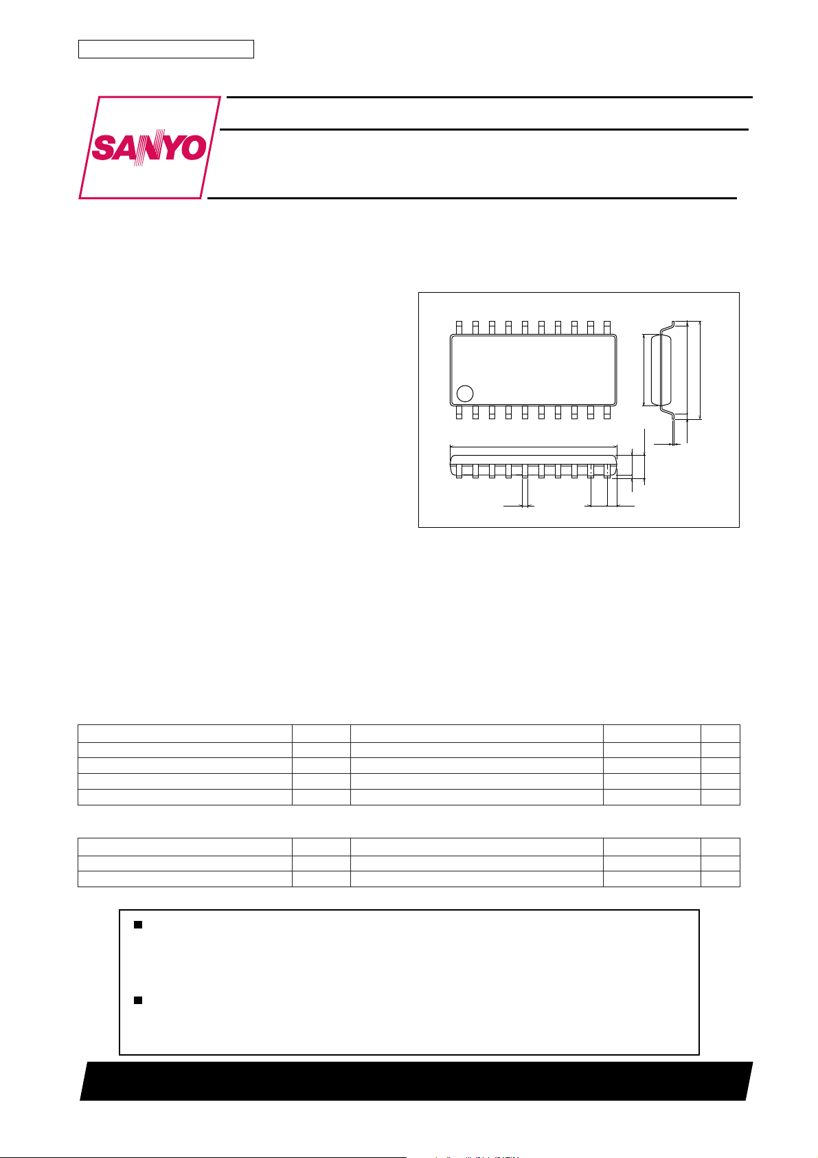
Package Dimensions
unit:mm
3036B-MFP20
20
1
0.35
[LA4571MB]
12.6
1.27
11
10
1.50.1
0.59
5.4
0.15
1.8 max
SANYO : MFP20
6.35
0.625
7.6
Specifications
Maximum Ratings at Ta = 25˚C
retemaraPlobmySsnoitidnoCsgnitaRtinU
egatlovylppuSV
noitapissidrewopelbawollAxamdP 004Wm
erutarepmetgnitarepOrpoT 57+ot02–
erutarepmetegarotSgtsT 521+ot04–
Recommended Operating Conditions at Ta = 25˚C
retemaraPlobmySsnoitidnoCsgnitaRtinU
egatlovylppuSV
egnaregatlovylppuSV
xam 5.4V
CC
CC
po 6.3ot8.1V
CC
40500TN (KT)/3271TS (US) No.3534–1/9
˚C
˚C
0.3V
Page 2
LA4571MB
Electrical Characteristics
Preamplifier and power amplifier at Ta = 25˚C, VCC=3.0V, f=1kHz, RL (pre)=10kΩ, RL (power)=16Ω,
0dBm at 0.775V unless otherwise noted
retemaraPlobmySsnoitidnoC
tnerrucylppustnecseiuQI
niagegatlovlatoTGV
OCC
T
k2.2=gR Ω V,IV0=7172Am
V
mBd5–=568617Bd
O
nimpytxam
Preamplifier at Ta = 25˚C, VCC=3.0V, f=1kHz, RL (pre)=10kΩ, RL (power)=16Ω, 0dBm at 0.775V unless otherwise
noted
retemaraPlobmySsnoitidnoC
niagegatlovpool-nepOGV
niagegatlovpool-desolCGV
egatlovtuptuomumixaMV
noitrotsidcinomrahlatoTDHT
egatlovesionnoisrevnoctupnIV
klatssorclennahCTC
noitcejerelppiRR
O
O
1
xamV,%1=DHT
1VO
IN
1
1r
V
V
mBd5–=0708Bd
O
mBd5–=04Bd
O
k2.2=gR Ω zHk02otzH02=htdiwdnab,3.10.2Vµ
k2.2=gR Ω enutzHk1,0608Bd
k2.2=gR Ω V,
V8.1=1.02.0V
CC
V,V8.1=
CC
r
)dradnatsBAN(Bd04=GV,V2.0=50.05.0%
zH001=f,mBd02–=0405Bd
nimpytxam
Power amplifier at Ta = 25˚C, VCC=3.0V, f=1kHz, RL (pre)=10kΩ, RL (power)=16Ω, 0dBm at 0.775V unless
otherwise noted
retemaraPlobmySsnoitidnoC
rewoptuptuOP
niagegatlovpool-desolCGV
noitrotsidcinomrahlatoTDHT
klatssorclennahCTC
egatlovesiontuptuOV
noitcejerelppiRR
ecnatsisertupnIR
egatlovtesffoCDtuptuOV
O
2
2PO
T
ON
2r
i
ffoCDO
%01=DHT3223Wm
V
V
mBd5–=528213Bd
O
Wm1=4.00.1%
R,mBd5–=
O
0=gR Ω zHk02otzH02=FPB,4204Vµ
0=gR Ω V,
0= Ω 0304Bd
V
V,zH001=f,Bd02–=
r
V8.1=5406Bd
CC
Note : The maximum and minimum values for the power amplifiers closed-loop voltage gain (VG2) increase by 1dB when the load resistance (RL) is
32Ω.
nimpytxam
sgnitaR
sgnitaR
sgnitaR
220383kΩ
09–09+Vm
tinU
tinU
tinU
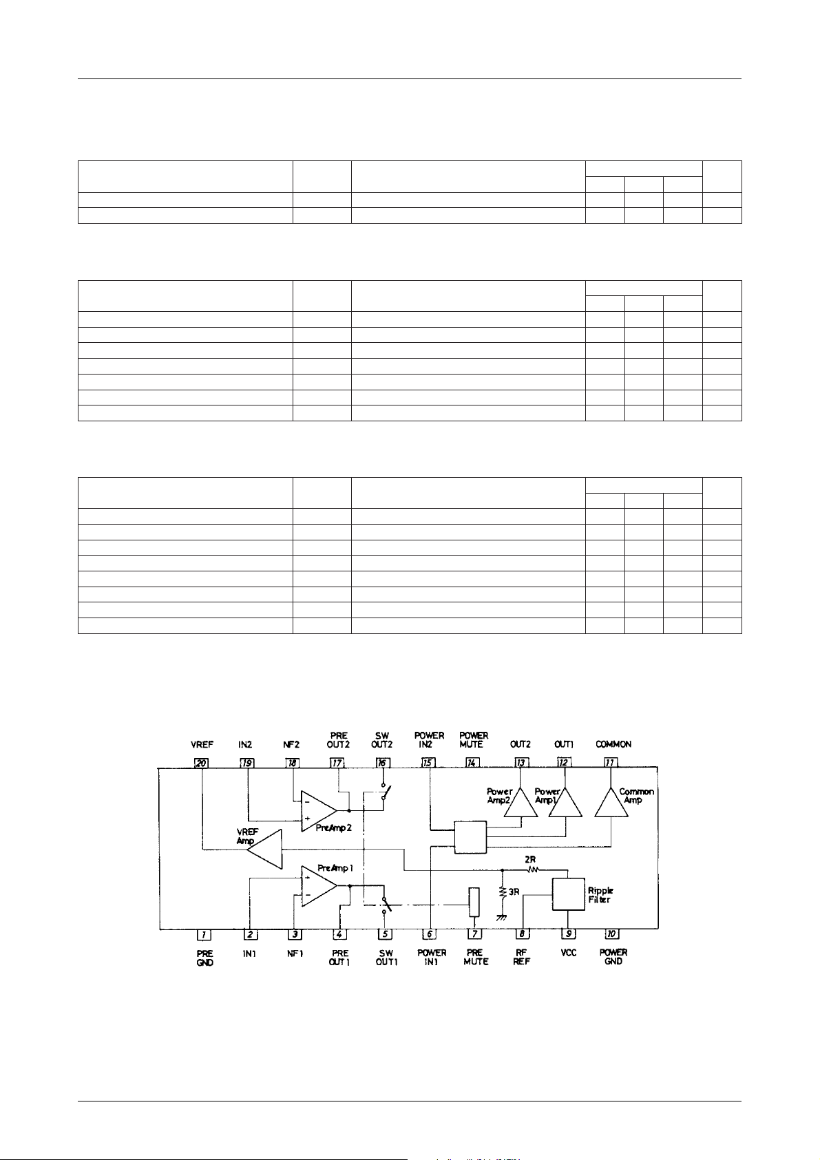
Block Diagram
No.3534–2/9
Page 3
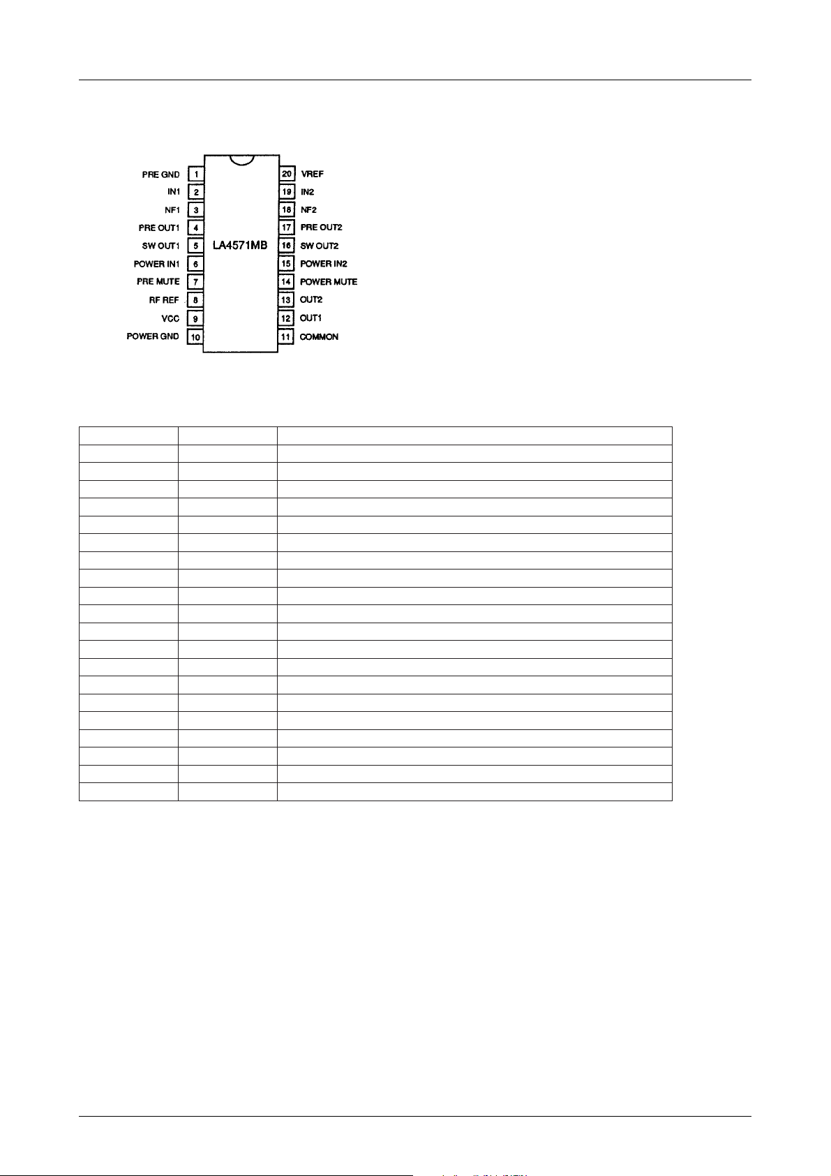
Pin Assignment
Pin Description
rebmuNemaNnoitpircseD
1DNGERPdnuorgreifilpmaerP
21NItupnireifilpmaerp1lennahC
31FNtupnikcabdeefevitagenreifilpmaerp1lennahC
41TUOERPtuptuoreifilpmaerp1lennahC
51TUOWSNIRtuptuodehctiwslortnoc-etumreifilpmaerp1lennahC ≥ k005 Ω
61NIREWOPR.tupnireifilpmarewop1lennahC
7ETUMERPlortnocetumreifilpmaerP
8FERFRnoitcennocroticapacretlif-elppiR
9V
01DNGREWOPdnuorgreifilpmarewoP
11NOMMOCtuptuoreifilpmanommoC
211TUOtuptuoreifilpmarewop1lennahC
312TUOtuptuoreifilpmarewop2lennahC
41ETUMREWOPlortnocetumreifilpmarewoP
512NIREWOPR.tupnireifilpmarewop2lennahC
612TUOWSR.tuptuodehctiwslortnoc-etumreifilpmaerp2lennahC
712TUOERPtuptuoreifilpmaerp2lennahC
812FNtupnikcabdeefevitagenreifilpmaerp2lennahC
912NItupnireifilpmaerp2lennahC
02FERVI.tuptuoreifilpmaegatlov-encerefeR
LA4571MB
Top view
≅ k03 Ω
NI
CC
egatlovylppuS
≅ k03 Ω
NI
≥ k005 Ω
NI
Aµ005±=
xam
No.3534–3/9
Page 4

Test Circuit
LA4571MB
Allowable power dissipation, Pd max – mW
Ambient temperature, Ta – °C
Pd max – Ta
VGO, VG – f
I
CCO
– mA
CCO
Quiescent supply current, I
Supply voltage, VCC – V
THD – V
– V
CC
O
Voltage gain, VG – dB
Frequency, f – Hz
Total harmonic distortion, THD – %
Output voltage, VO – V
No.3534–4/9
Page 5

LA4571MB
– dB
GO
Open-loop voltage gain, V
VGO – V
Supply voltage, VCC – V
CC
CT – f
– µV
max – V
Maximum output voltage, V
NO
VO max – V
O
Supply voltage, VCC – V
VNO – V
CC
CC
Channel crosstalk, CT – dB
Frequency, f – Hz
VO – f
– dBm
O
Output level, V
Frequency, f – Hz
Vref – I
Output noise voltage, V
Supply voltage, VCC – V
SVRR – V
Supply voltage rejection ratio, SVRR – dB
O
Supply voltage, VO – V
CC
Reference voltage, Vref – V
Output current, IO – mA
No.3534–5/9
Page 6

LA4571MB
VDC – V
– V
DC
DC voltage, V
Supply voltage, VCC – V
VO max – V
max – V
O
CC
Channel crosstalk, CT – dB
CC
CT – f
Frequency, f – Hz
THD – V
CC
Maximum output voltage, V
Voltage gain, VG – dB
Supply voltage, VCC – V
VG – f
Frequency, f – Hz
VG – V
CC
Total harmonic distortion, THD – %
Total harmonic distortion, THD – %
Supply voltage, VCC – V
THD – P
Output power, PO – mW
THD – P
O
O
Voltage gain, VG – dB
Supply voltage, VCC – V
Total harmonic distortion, THD – %
Output power, PO – mW
No.3534–6/9
Page 7

LA4571MB
VNO – V
– µV
NO
Output noise voltage, V
Supply voltage, VCC – V
CC
Functional Decription (channl 1 only)
Tape Head Preamplifier
Tape head signal source are connected to the noninverting input of the op-amp, negative feedback preamplifier.
When PRE MUTE is open, the preamplifier output is
connected to SW OUT1, and when PRE MUTE is HIGH
(VCC ±0.2V at 60µA input current), SW OUT1 is open.
This can be used to switch, or mute, the preamplifier
output.
Supply voltage rejection ratio, SVRR – dB
SVRR – V
Supply voltage, VCC – V
CC
The internal circuit of the PRE MUTE pin is shown in
the following figure.
The output pins, PRE OUT1 and SW OUT1, can both
drive a 10kΩ load resistance.
The preamplifier input pin, IN1, the negative feedback
input pin, NF1, and the output pin, PRE OUT, are
biased at 1.8V.
Power Amplifier
The power amplifier stage comprises an amplifier for
each channel and a common amplifier. The power
amplifier outputs are connected internally by 60Ω
resistors to prevent oscillation, as shown in the following figure.
When POWER MUTE is LOW (less than 0.3V at
2.5µA input current), the power amplifier output signal
is muted. The power amplifier mute release time is set
by an external capacitor.
No.3534–7/9
Page 8

LA4571MB
The internal circuit of the POWER MUTE pin is shown
in the following figure.
The power amplifier input pin, POWER IN1, is biased at
1.8V, and the output pins at 1.2V
Design Notes
The preamplifier inputs should be connected to V
through a 2.2kΩ resistor if there is no tape head input
signal source.
The mute release time capacitor of the power amplifier
should be between 1.0 and 4.7µF. For VCC=3.0V and
C=2.2µF, the mute release time is 0.7s.
The ripple rejection ratio setting capacitor should be
between 2.2 and 33µF. For 2.2µF, the ripple rejection
ratio is 35dB, and for 22µF, it is 55dB.
When the output amplifier turns OFF, the protection
circuit shown in the following figure detects the falling
supply voltage and then mutes the power amplifier to
protect the device.
REF
Reference Voltage
The input to the voltage reference amplifier is a
voltage divided level from the supply voltage ripple
filter. The referecne voltage is given by 0.6 × VCC.
The supply voltage ripple filter requires the connection
of an external filter capacitor to RF REF. A large
capacitance results in a high ripple rejection ratio.
Noise filtering is achieved by the addition of a single
capacitor to VREF. Since the reference voltage amplifier has a buffered output, this capacitor can be as low
as 1µF.
Sample Application Circuit
No.3534–8/9
Page 9

LA4571MB
Specifications of any and all SANYO products described or contained herein stipulate the performance,
characteristics, and functions of the described products in the independent state, and are not guarantees
of the performance, characteristics, and functions of the described products as mounted in the customer's
products or equipment. To verify symptoms and states that cannot be evaluated in an independent device,
the customer should always evaluate and test devices mounted in the customer's products or equipment.
SANYO Electric Co., Ltd. strives to supply high-quality high-reliability products. However, any and all
semiconductor products fail with some probability. It is possible that these probabilistic failures could
give rise to accidents or events that could endanger human lives, that could give rise to smoke or fire,
or that could cause damage to other property. When designing equipment, adopt safety measures so
that these kinds of accidents or events cannot occur. Such measures include but are not limited to protective
circuits and error prevention circuits for safe design, redundant design, and structural design.
In the event that any or all SANYO products(including technical data,services) described or
contained herein are controlled under any of applicable local export control laws and regulations,
such products must not be exported without obtaining the export license from the authorities
concerned in accordance with the above law.
No part of this publication may be reproduced or transmitted in any form or by any means, electronic or
mechanical, including photocopying and recording, or any information storage or retrieval system,
or otherwise, without the prior written permission of SANYO Electric Co. , Ltd.
Any and all information described or contained herein are subject to change without notice due to
product/technology improvement, etc. When designing equipment, refer to the "Delivery Specification"
for the SANYO product that you intend to use.
Information (including circuit diagrams and circuit parameters) herein is for example only ; it is not
guaranteed for volume production. SANYO believes information herein is accurate and reliable, but
no guarantees are made or implied regarding its use or any infringements of intellectual property rights
or other rights of third parties.
This catalog provides information as of April, 2000. Specifications and information herein are subject to
change without notice.
PS No.3534–9/9
 Loading...