

Page 1
Any and all SANYO products described or contained herein do not have specifications that can handle
applications that require extremely high levels of reliability, such as life-support systems, aircraft’s
control systems, or other applications whose failure can be reasonably expected to result in serious
physical and/or material damage. Consult with your SANYO representative nearest you before using
any SANYO products described or contained herein in such applications.
SANYO assumes no responsibility for equipment failures that result from using products at values that
exceed, even momentarily, rated values (such as maximum ratings, operating condition ranges,or other
parameters) listed in products specifications of any and all SANYO products described or contained
herein.
Monolithic Linear IC
240mW AF Power Amplifier
Ordering number:ENN1161D
LA4510
SANYO Electric Co.,Ltd. Semiconductor Company
TOKYO OFFICE Tokyo Bldg., 1-10, 1 Chome, Ueno, Taito-ku, TOKYO, 110-8534 JAPAN
Applications
• Especially suited for use in 3V micro cassette recorder,
mini cassette recorder, headphone stereo applications.
Features
• Operating supply voltage range : 2 to 5V.
• Low current dissipation (7mA typ/VCC=3V).
• Output power :
240mW typ at VCC=3V, RL=4Ω, THD=10%
40mW typ at VCC=3V, RL=32Ω, THD=10%
• Built-in muting circuit to be operated at the time of power
switch ON capable of varying starting time and making
pop noise low.
• Soft clipping.
Specifications
Absolute Maximum Ratings at Ta = 25˚C
retemaraPlobmySsnoitidnoCsgnitaRtinU
egatlovylppusmumixaMV
tnerructuptuomumixaM
noitapissidrewopelbawollAxamdP 007Wm
erutarepmetgnitarepOrpoT 06+ot01–
erutarepmetegarotSgtsT 051+ot55–
xam 0.6V
CC
IOkaep
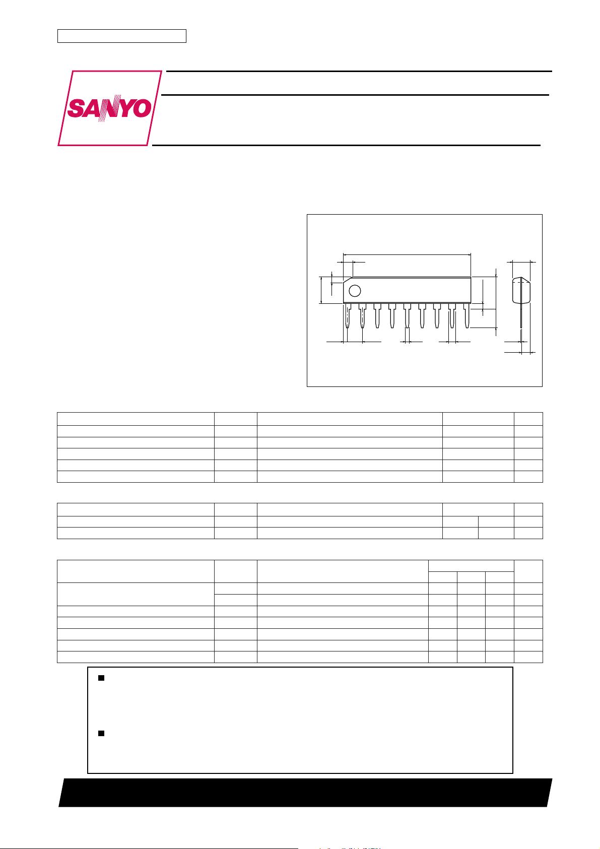
Package Dimensions
unit:mm
3017C-SIP9
[LA4510]
1.5
4.8
1.0
1
0.99
2.54
22.3
0.5
0.51min
9
1.3
SANYO : SIP9
3.0
5.7max
3.2
0.25
1.35
075Am
˚C
˚C
Operating Conditions at Ta = 25˚C
retemaraPlobmySsnoitidnoCsgnitaRtinU
egatlovylppusdednemmoceRV
ecnatsiserdaoldednemmoceRR
CC
L
0.35.4V
23ot423ot8
Operating Characteristics at Ta = 25˚C, VCC=3.0V, RL=4Ω, f=1kHz, See Sample Application Circuit 1.
retemaraPlobmySsnoitidnoC
I
1langisoN721Am
tnerructnecseiuQ
niagegatloVGVR1001= Ω 245484Bd
rewoptuptuOP
noitrotsidcinomrahlatoTDHTPOWm001=4.05.1%
egatlovesiontuptuOV
egatlovelppirtuptuOprVf,0=gR
OCC
I
OCC
O
ON
2V,langisoN
%01=DHT002042Wm
k1=gR Ω zHk02otzH02=WB,2.05.0Vm
R
V5.4=5.851Am
CC
V,zH001=
Vm05=7.0Vm
R
21500TN (KT)/41594HK/O147KI/2126KI/4225MW/D132KI, TS No.1161–1/8
nimpytxam
Ω
sgnitaR
tinU
Page 2
Equivalent Circuit Block Diagram
Sample Application Circuit 1 : Speaker load
LA4510
Description of external parts
C1 (1µF) · Input capacitor (Coupling capacitor for input signal)
Decreasing the capacitance value lowers the frequency response at low frequencies.
C2 (22µF) · Feedback capacitor (Bypass of feedback signal)
Decreasing the capacitance value lowers the frequency response at low frequencies ; increasing the
capacitance value makes the starting time latar.
C3 (4.7µF) · Muting capacitor
Decreasing the capacitance value makes the starting time earlier ; removing C3 causes pop noise.
Increasing the capacitance value makes the starting time later.
C4 (220pF) · Phase compensation capacitor (Phase compensation by local feedback) Decreasing the capacitance
value causes the frequency response to extend at high frequencies, and thereby oscillation is liable to
occur. Increasing the capacitance value worsens distortion factor at high frequencies.
C5 (0.47µF) · Oscillation blocking capacitor
Decreasing the capacitance value causes oscillation to liable to occur. Using an ordinary electrolytic
capacitor may cause oscillation to occur at a low temperature. Use a tantalum or alsicon electrolytic
capacitor that is good in temperature characteristic.
C6 (470µF) · Output capacitor (Cutoff of DC to speaker)
Decreasing the capacitanc value causes insufficient power at low frequencies.
C7 (220µF) · Bootstrap capacitor (Feedback from output stage)
Decreasing the capacitance value causes insufficient power at low frequencies, especially when
voltage is reduced.
C8 (220µF) · Power capacitor (Drop in power impedance)
Decreasing the capacitance value causes motor noise, etc. to be entered easily. Removing C8 may
cause oscillation to occur.
C9 (47µF) · Capacitor for ripple filter (Filter for bias voltage)
Decreasing the capacitance value causes the circuit to be subjected to the influence of power supply,
and thereby ripple is liable to occur.
ri (100Ω) · Feedback resistor (Setting of voltage gain)
Decreasing the resistance value increases voltage gain, but worsens distortion factor, and thereby gain
varies. Increasing the resistance value causes oscillation to liable to occur.
No.1161–2/8
Page 3
LA4510
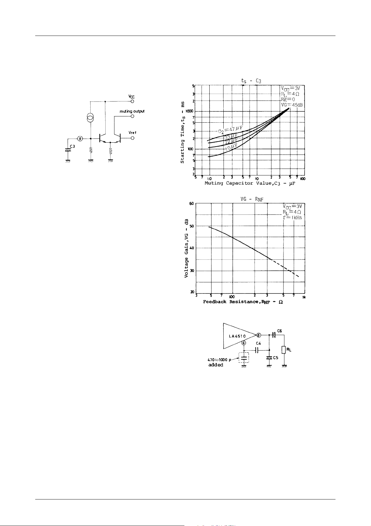
Setting of Starting Time
The LA4510 contains a muting circuit to be operated at the time of power switch ON/OFF. Thus, pop noise coming
from power amplifier and preamplifier is rejected. The starting time depends on the capacitance value of feedback
capacitor C2 as well as muting capacitor (C3).
V oltage Gain
Voltage gain depends on the ratio of internal resistance value (20kΩ) to external resistance value (R1).
However, since setting of open loop voltage gain is a
little on the low side (62dB) due to soft cliping, it is
not recommendable to use the IC at a voltage gain
greater than recommended. If the IC is used at a
voltage gain less than recommended, take care not to
cause oscillation to occur.
Action to Prevent Oscillation
If oscillation occurs, check C5. The larger the capacitance value is or the smaller the value of tan δ is if the
capacitance value is the same, C5 acts more effectively against oscillation. Using an electrolytic
capacitor as C5 may cause oscillation to occur at a
low temperature.
It is recommendable to use a tantalum or alsicon electrolytic capacitor that is good in temperature characteristic. For
oscillation that occurs at a decreased voltage gain, increase the capacitance value of C4. If it is impossible for C4, C5
to act effectively against oscillation, add a ceramic capacitor of 470 to 1000pF across pin (4) and GND. In this case,
distortion factor at high frequencies worsens to some extent.
No.1161–3/8
Page 4

LA4510
Removal of Bootstrap Capacitor
In applications where more power than required is availabel (approximately 60% of rating), it is possible to remove
bootstrap capacitor C7 (pin (7)-to-pin (8) short). However, since this causes clipping unbalance to occur, this unbalance must be compensated by use of a resistor and a diode. A simple compensation method is shown below. This
method makes it possible to attain clipping balance at a certain supply voltage only.
No.1161–4/8
Page 5

LA4510
No.1161–5/8
Page 6

LA4510
Sample Application Circuit 2 : Headphone load
No.1161–6/8
Page 7

Sample Application Circuit 3 : Bridge
LA4510
*Note) · For C10, C11, use tantalum or
alsicon electrolytic capacitor.
· If oscillation occurs, add C14
(0.1 to 0.2µ ceramic capacitor).
Proper Cares in Using IC
· Maximum ratings
If the IC is used in the vicinity of the maximum ratings, even a slight variation in conditions may cause the maximum
ratings to be exceeded, thereby leading to breakdown. Allow an ample margin of variation for supply voltage, etc. and
use the IC in the range where the maximum ratings are not exceeded.
· Pin-to-pin short
If power is applied when the space between pins is shorted, breakdown or deterioration may occur. When mounting the
IC on the board or applying power, make sure that the space between pins is not shorted with solder, etc.
· Printed circuit pattern
When designing the printed circuit pattern, make the power supply, output, and ground lines thick and short and arrange
the pattern and parts so that no feedback loop is formed between input and output. Place power capacitor C8, oscillation
blocking capacitors C4, C5 as close to IC pins as possible to prevent oscillation from occurring. Refer to the sample
printed circuit pattern.
No.1161–7/8
Page 8

LA4510
Specifications of any and all SANYO products described or contained herein stipulate the performance,
characteristics, and functions of the described products in the independent state, and are not guarantees
of the performance, characteristics, and functions of the described products as mounted in the customer's
products or equipment. To verify symptoms and states that cannot be evaluated in an independent device,
the customer should always evaluate and test devices mounted in the customer's products or equipment.
SANYO Electric Co., Ltd. strives to supply high-quality high-reliability products. However, any and all
semiconductor products fail with some probability. It is possible that these probabilistic failures could
give rise to accidents or events that could endanger human lives, that could give rise to smoke or fire,
or that could cause damage to other property. When designing equipment, adopt safety measures so
that these kinds of accidents or events cannot occur. Such measures include but are not limited to protective
circuits and error prevention circuits for safe design, redundant design, and structural design.
In the event that any or all SANYO products(including technical data,services) described or
contained herein are controlled under any of applicable local export control laws and regulations,
such products must not be exported without obtaining the export license from the authorities
concerned in accordance with the above law.
No part of this publication may be reproduced or transmitted in any form or by any means, electronic or
mechanical, including photocopying and recording, or any information storage or retrieval system,
or otherwise, without the prior written permission of SANYO Electric Co. , Ltd.
Any and all information described or contained herein are subject to change without notice due to
product/technology improvement, etc. When designing equipment, refer to the "Delivery Specification"
for the SANYO product that you intend to use.
Information (including circuit diagrams and circuit parameters) herein is for example only ; it is not
guaranteed for volume production. SANYO believes information herein is accurate and reliable, but
no guarantees are made or implied regarding its use or any infringements of intellectual property rights
or other rights of third parties.
This catalog provides information as of February, 2000. Specifications and information herein are subject
to change without notice.
PS No.1161–8/8
 Loading...