

Page 1
Any and all SANYO products described or contained herein do not have specifications that can handle
applications that require extremely high levels of reliability, such as life-support systems, aircraft’s
control systems, or other applications whose failure can be reasonably expected to result in serious
physical and/or material damage. Consult with your SANYO representative nearest you before using
any SANYO products described or contained herein in such applications.
SANYO assumes no responsibility for equipment failures that result from using products at values that
exceed, even momentarily, rated values (such as maximum ratings, operating condition ranges,or other
parameters) listed in products specifications of any and all SANYO products described or contained
herein.
Monolithic Linear IC
12W AF Power Amplifier
for Car Radio, Car Stereo
Ordering number:ENN2660B
LA4460N, 4461N
SANYO Electric Co.,Ltd. Semiconductor Company
TOKYO OFFICE Tokyo Bldg., 1-10, 1 Chome, Ueno, Taito-ku, TOKYO, 110-8534 JAPAN
Features
• High gain of 51dB typ. and high power output of 12W
typ.
• Possible to delete output and bootstrap capacitors, this
encourages cost and space reductions due to external parts
reduction.
• Reduced external components (8 pieces recommended, 6
pieces minimum).
• Almost no pop noises heard during power on or off operation.
• Soft tonal quality in saturated power output.
• Low distortion over low to high ranges of the audio frequencies.
• Low residual noises (Rg=0).
• Good operation conditions because of SIP (single ended
pins) package having been employed for the LA4460N.
• All pin terminal layouts of the LA4461N are reversed for
easy stereo PC board pattern arrengement.
• Two ground terminals for pre-amplifier and power amplifier are provided for easy PC board pattern arrangement
and for stabilizing distortion chracteristics depending on
signal source impedance.
• Voltage gain is fixed at 51dB, however, lowering the gain
is possible by adding a resistor.
• IC is not damaged, if it is connected reversely.
• Audio muting functions (AC mute & DC mute) are
equipped.
• Several protection circuits are installed, including :
a. Thermal protection circuit.
b. Overvoltage & surge voltage protection circuit.
c. Load short-circuit current limiting protection circuit.
d. Output pins DC short-circuit protection circuit.
(grounding protection between OUT & GND, and
speaker protection provided.)
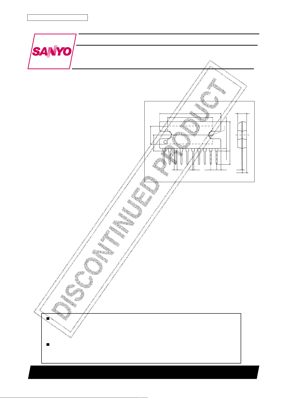
Package Dimensions
unit:mm
3024A-SIP10H
[LA4460N, 4461N]
27.0
20.0
8.4
7.0
1.4
0.5
2.54
101
4.0
R1.7
11.8
13.2max
6.0
1.0min
2.07
SANYO : SIP10H
0.4
2.0
21500TN (KT)/90196RM/D187KI, TS No.2660–1/12
Page 2
LA4460N, 4461N
Specifications
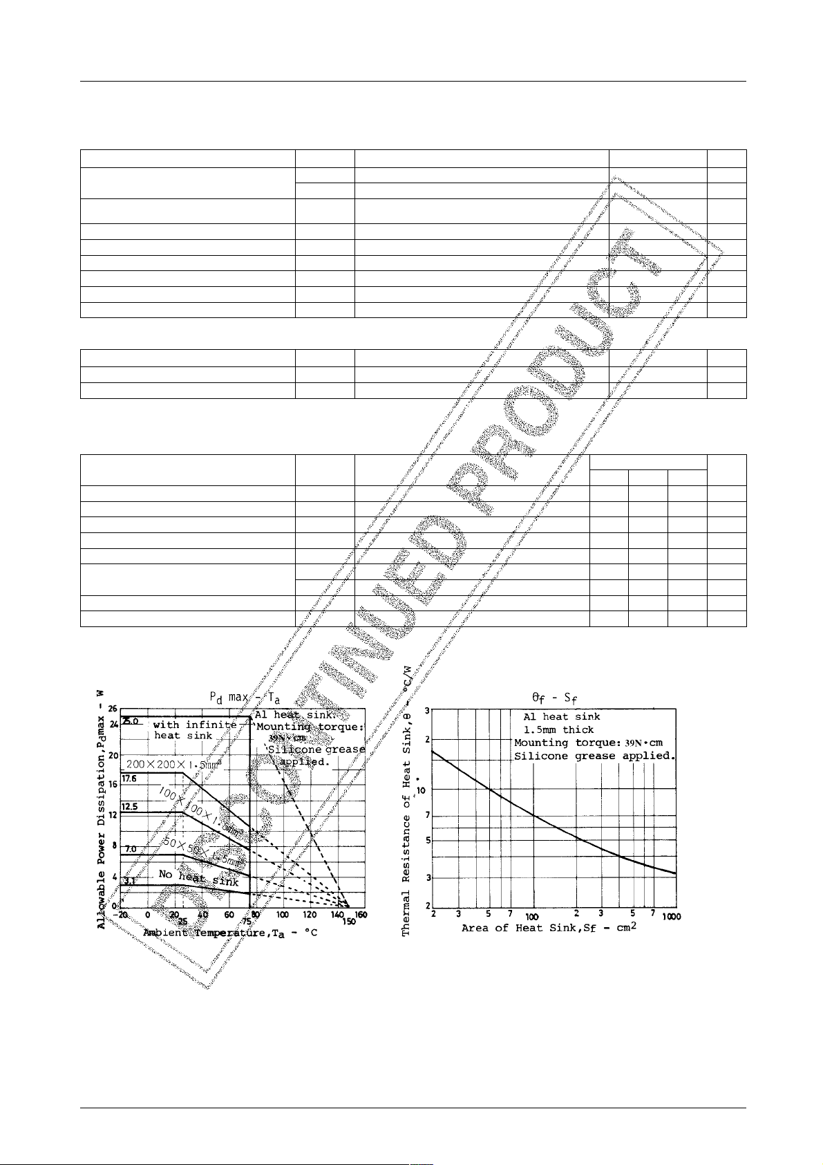
Absolute Maximum Ratings at Ta = 25˚C
retemaraPlobmySsnoitidnoCsgnitaRtinU
egatlovylppusmumixaM
tnerrucylppuSI
tnerructuptuOI
egatlovylppusegruSegrusVt≤ s2.0 05V
noitapissidrewopelbawollAxamdP 52W
ecnatsiserlamrehtegakcaP
erutarepmetgnitarepOrpoT 57+ot02–
erutarepmetegarotSgtsT 051+ot04–
V
V
Recommended Operating Conditions at Ta = 25˚C
retemaraPlobmySsnoitidnoCsgnitaRtinU
egatlovylppusdednemmoceRV
ecnatsiserdaoLR
1xam)s03(tnecseiuQ 52V
CC
2xamlangishtiw 81V
CC
kaep
01
7I,9
θ c-j
CC
L
ylno
kaepytudeulavsuoenatnatsnI ≤ htdiweslup,%5 ≤ sm15.4A
Tc=75˚C, See Pd max – Ta graph.
ytudeulavsuoenatnatsnI ≤ htdiweslup,%5 ≤ ni-wolfsm1
5.4A
3
˚C/W
˚C
˚C
2.31V
Ω
8ot4
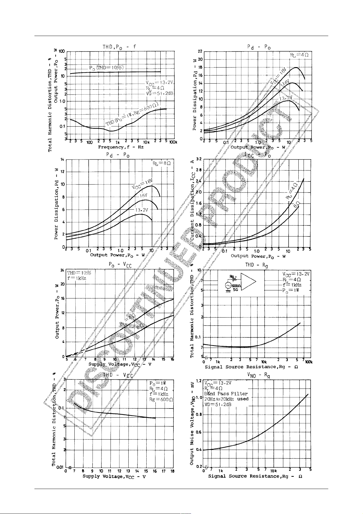
Operating Characteristics at Ta = 25˚C, VCC=13.2V, RL=4Ω, f=1kHz, Rg=600Ω, with 100×100×1.5mm
Al heat sink, See specified Test Circuit
retemaraPlobmySsnoitidnoC
tnerructnecseiuQI
niagegatloVGV.tiucricdednemmocerdeificepsta,pooldesolc941535Bd
rewoptuptuOP
noitrotsidcinomrahlatoTDHTPOW1=1.00.1%
ecnatsisertupnIr
egatlovesiontuptuO
egatlovtesffotuptuOffoV003– 003+Vm
)CA(noitaunettagnituMA
(Note) : For DC muting, ATT=∞
nimpytxam
OCC
O
i
VON1retlifssap-dnab,zHk02otzH02=f,0=gR4.00.1Vm
VON2k01=gR Ω retlifssap-dnab,zHk02otzH02=f,6.00.2Vm
TT
%01=DHT0121W
V
O
V,mBd0=
V9=83Bd
M
sgnitaR
56021Am
1203kΩ
3
tinU
No.2660–2/12
Page 3

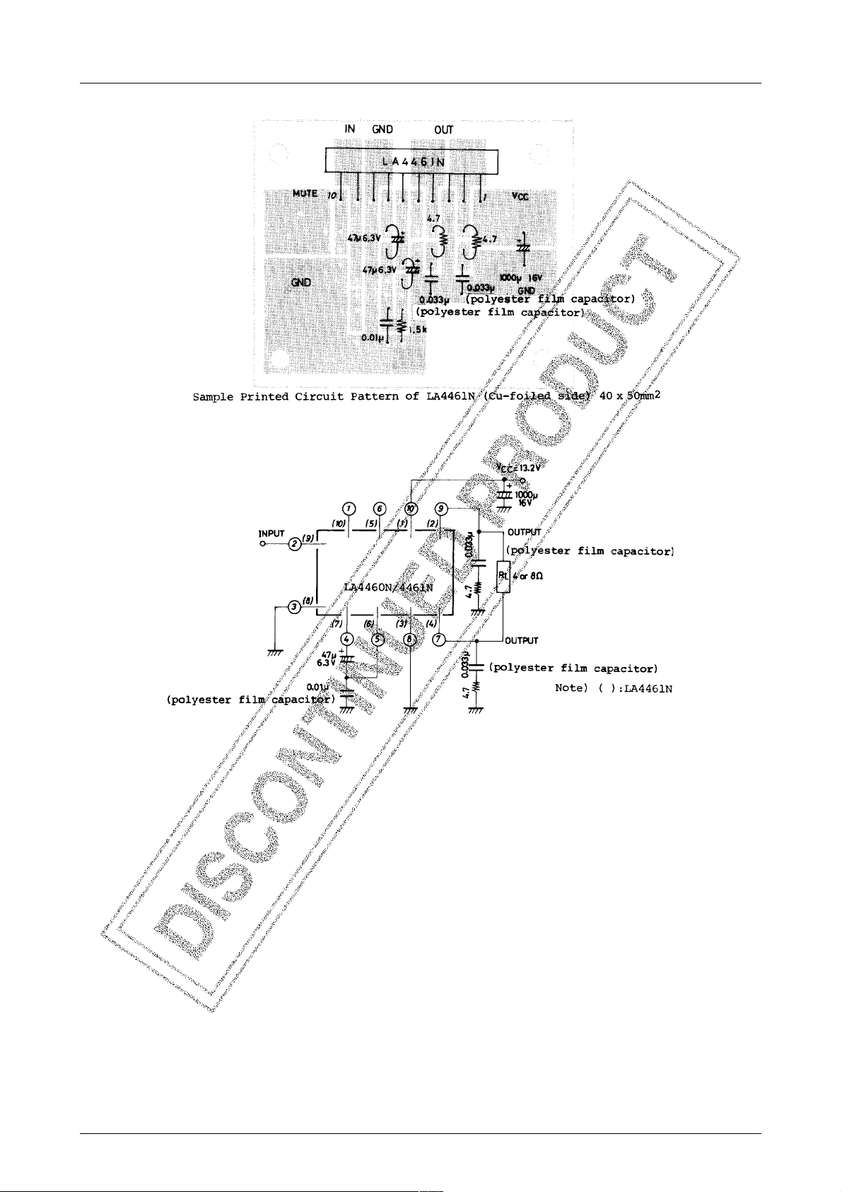
Equivalent Circuit Block Diagram
LA4460N, 4461N
Sample Application Circuit 1 : Recommended Circuit
No.2660–3/12
Page 4
LA4460N, 4461N
Sample Application Circuit 2 : An Example with Minimum Parts
Functional Description on the External Parts
Recommended number of the external parts for the LA4460N/4461N is 8 as shown in the Sample Application Circuit 1.
Namely they are :
· Feedback capacitors 2 pieces 4.7µF/6.3V×2
· Starting time adjustmant resistor 1 pieace 1.5kΩ
· Oscillation compensation capacitor 1 piece 0.01µF
· Oscillation compensation C · R 4 pieces 0.033µF×2, 4.7Ω×2
a) Feedback capacitor CNF
This relates to a low range cutoff frequency f
decreasing C
NF
.
b) Oscillation compensation capacitor C
X
, and fL lowers with increasing value of the ‘CNF and increases with
L
Signals are applied from the non-inverted NF ter minal to the inverted NF terminal through the two CNF capacitors. It
is recommended to connect the oscillation compensation capacitor C
capacitors (minus side of C
) and GND. As a rule a polyester film capacitor is recommended, but a ceramic type
NF
=0.01µF between the floating junction of the
X
may be used if a PC board shows good circuit stability.
No.2660–4/12
Page 5

LA4460N, 4461N
c) Starting time adjustment resistor R
X
The purpose of the RX is to adjust the starting time ts, and a resistor of 1.5kΩ is used. In this case, a rising DC locus
as shown below will be obtained at the output terminals.
The circuit has been set to provide signals about 0.4µs. after the power is turned on. Though the ts will increase with
decreasing R
, the total output across the load will be decreased, since the signal flowing to the non-inv erted side will
X
flow into the ground through the RX. Contrarily, increasing the RX to RX=∞ as shown in the Sample Application
Circuit 2, the ts reduces to zero s., and the rising locus as shown below will be obtained.
d) Oscillation compensation CR across the load
To prevent parasitic oscillation, it is recommended to connect 0.033µF plus 4.7Ω between each channel output termi-
nal and GND. (As a rule the capacitor should be a polyester film capacitor.) This measure against the oscillation may
be replaced with the methods as shown below, depending upon the stability of PC boards used.
Note :
· Check for oscillation at low temperatures.
· Check for oscillation on stereo PC boards.
· Do not use shielded wires for output cords.
Note :
· Check for oscillation at low temperatures.
· Use 8Ω load resistor.
· Do not use shielded wires for output cords.
· L should be higher than 0.3µH.
(Removal of oscillation compensation CR)
Coil used
Air core Inner diameter : 8ø Number of turns : 6 turns
Wire size : UEW 1.5 Winding method : Solenoid (0.3µH)
Above examples can be applied to the Sample Application Circuits 1, 2.
Features of IC System and Roles of the Remaining Pin Terminals
· Since a zero-bias design is introduced into the input circuit to keep the input potential at about zero by employing PNP
in the input circuit, an input coupling capacitor can be removed for direct connection. Howe v er, when noises caused by
a DC current flowing to a volume control circuit or the input circuit causes problems, connect a capacitor in series with
the input circuit.
· To prevent damage or deterioration of the IC due to the load short-circuited, a load short-circuit current limiting type
protection circuit has been provided.
However, when making the load short-circuit test, always mount the IC on the specified heat sink.
· A circuit which prevents pop noise caused by the po wer on-off operation is also provided, thereby reducing the offset
voltage and protecting speaker systems against damage.
Continued on next page.
No.2660–5/12
Page 6

LA4460N, 4461N
Continued from preceding page.
· Soft clipping characteristics are accomplished by lowering the open loop voltage gain and reducing the amount of
feedback to reduce undesired radiation to radio frequency circuits and to increase the circuit stability. The distortion
deterioration resulted from the decreased amount of feedback will be avoided by using a unique distortion reduction
circuit, thus 0.1% typ. will be assured.
· A capacitor for oscillation compensation is included inside the IC as a method of reducing external parts.
The capacitance is 30pF and this determines the cutoff frequency f
· To reduce variations of the voltage gain, a feedback resistor R
RNF=53Ω, Rf=20kΩ
when R
VG=20log (dB)
NF
’=0
R
f
R
NF
(–3dB point) of the high range (fH≈30kHz).
H
is also built-in, and the voltage gain is fix ed to 51dB.
NF
when R
’ is used
NF
VG=20log (dB)
RNF +
R
f
R
’
NF
2
Howev er the v oltage gain will be decreased by adding a resistor R
’, where the RNF’ is the resistor to be connected to
NF
the pin 4. (In the Sample Application Circuit 2, the gain adjustment will be made with the resistor connected to either
pin 4 or 5.)
· Two ground pin terminals are provided, one for the preamplifier and the other for the power amplifier. Accordingly,
stability of the IC is increased, especially, distortion deterioration phenomenon caused by increased signal source
impedance Rg is improved and a flat response will be obtained.
· An overvoltage protector circuit is included to protect the IC from damage when a sur ge voltage is applied to the po wer
line. The overvoltage is set at 25V, however, the circuit can resist 50V for giant pulse surge of 200ms.
· For OCL connections, a DC short-circuit protection circuit is required. Therefore a grounding protection circuit which
endures against the OUTPUT-GND short-circuit is provided. Since consideration is giv en to the of fset caused by shortcircuit or releasing the short-circuit both the speaker and the IC can be protected.
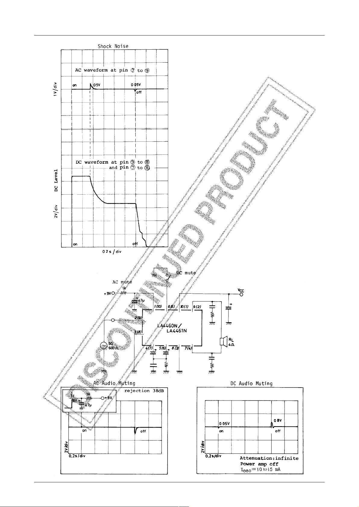
· When adding an audio muting circuit in each application circuit, refer to the illustration below.
6V≤V
M≤VCC
Recommended VM=9V
ATT=38dB (Rg=600Ω)
Flow-in current I
is calculated as shown below.
O
– V
V
M
IO=
BE
R
1
To increase muting attenuation, connect a resistor of 5.6kΩ in series with the input circuit, then the attenuation will be
increased to 55dB. It should be noted that adding an input capacitor will increase pop noise when the AC muting is
operated. Pop noise can be reduced by increasing the value of R
and C1.
1
No.2660–6/12
Page 7

LA4460N, 4461N
Pin Voltage (unit : V)
N0644AL 123456789 01
N1644AL01 987654321
noitcnuF
egatlov
CA
oiduA
TUPNI
gnituM
niptnecseiuQ
060.008.28.26.56.606.62.31
Much data on general characteristics are given for the Sample Application 1, but these data can be also applied to the
Sample Application 2 because of no characteristic changed. However, the data on “Pop noise at power turned on”,
“Starting time t
” and “DC muting” are shown for only the Sample Application 1. For the same characteristics to be
s
applied to the Sample Application 2, refer to 1-C on page 4.
NON
erP
VNI
DNG
FN
CD
VNI
TUO
VNI
oiduA
TUO
gnituM
NON
rewoP
VNI
V
DNG
CC
TUO
No.2660–7/12
Page 8
LA4460N, 4461N
No.2660–8/12
Page 9

LA4460N, 4461N
No.2660–9/12
Page 10
LA4460N, 4461N
AC, DC Audio Muting Test Circuit
No.2660–10/12
Page 11

Sample Application Circuit 3 :
Note ) In case where the LA3161 is used,
Rb and Cb must be changed. (Refer
to the LA3161 catalog.)
LA4460N, 4461N
Example of oscillation compensation where feedthrough capacitors and used at the output terminals.
Coil used :
Air core Inner diameter : 8ø
Number of turns : 6 turns
Wire size : UEW 1.5
Winding method : solenoid (0.3µH)
Connect each coil, L1 and L2, in series with each output terminal, where L
1=L2
.
No.2660–11/12
Page 12

LA4460N, 4461N
Cy is a semiconductor ceramic capacitor (B.C.) of 0.5µF.
Note on LA4460N/4461N Usage
· Maximum ratings
When the IC is used in the vicinity of the maximum ratings, a minor change in the conditions could result in exceeding
the maximum ratings, and this may lead the IC to damege. Therefore suff icient precautions should be taken in this case.
· Short-circuiting among pin terminals
Damage or deterioration could result if the power is turned on with pins short-circuited. Therefore always make sure
the pins are not bridged by solder, etc. when mounting the IC on the PC board and turn the power on.
· Printed circuit board
In designing a printed circuit board, refer to the foil pattern example attached. Also mak e sure no feedback loop exists
between the input and output circuits.
· Others
The IC is an OCL type power IC in which a bridge connection is made. Care should be given to the ground connections
of the test equipment so that the ground of the test equipment (VTVM, distortion analyzer, oscilloscope, etc.) connected to the output terminals are not commonly connected to those of the test equipment connected to the input
terminals.
Specifications of any and all SANYO products described or contained herein stipulate the performance,
characteristics, and functions of the described products in the independent state, and are not guarantees
of the performance, characteristics, and functions of the described products as mounted in the customer's
products or equipment. To verify symptoms and states that cannot be evaluated in an independent device,
the customer should always evaluate and test devices mounted in the customer's products or equipment.
SANYO Electric Co., Ltd. strives to supply high-quality high-reliability products. However, any and all
semiconductor products fail with some probability. It is possible that these probabilistic failures could
give rise to accidents or events that could endanger human lives, that could give rise to smoke or fire,
or that could cause damage to other property. When designing equipment, adopt safety measures so
that these kinds of accidents or events cannot occur. Such measures include but are not limited to protective
circuits and error prevention circuits for safe design, redundant design, and structural design.
In the event that any or all SANYO products(including technical data,services) described or
contained herein are controlled under any of applicable local export control laws and regulations,
such products must not be exported without obtaining the export license from the authorities
concerned in accordance with the above law.
No part of this publication may be reproduced or transmitted in any form or by any means, electronic or
mechanical, including photocopying and recording, or any information storage or retrieval system,
or otherwise, without the prior written permission of SANYO Electric Co. , Ltd.
Any and all information described or contained herein are subject to change without notice due to
product/technology improvement, etc. When designing equipment, refer to the "Delivery Specification"
for the SANYO product that you intend to use.
Information (including circuit diagrams and circuit parameters) herein is for example only ; it is not
guaranteed for volume production. SANYO believes information herein is accurate and reliable, but
no guarantees are made or implied regarding its use or any infringements of intellectual property rights
or other rights of third parties.
This catalog provides information as of February, 2000. Specifications and information herein are subject
to change without notice.
PS No.2660–12/12
 Loading...