

Sanyo LA4270 Specifications
Any and all SANYO products described or contained herein do not have specifications that can handle
applications that require extremely high levels of reliability, such as life-support systems, aircraft’s
control systems, or other applications whose failure can be reasonably expected to result in serious
physical and/or material damage. Consult with your SANYO representative nearest you before using
any SANYO products described or contained herein in such applications.
SANYO assumes no responsibility for equipment failures that result from using products at values that
exceed, even momentarily, rated values (such as maximum ratings, operating condition ranges,or other
parameters) listed in products specifications of any and all SANYO products described or contained
herein.
Monolithic Linear IC
6W Dual-Channel AF Power Amplifier
Ordering number:ENN1724D
LA4270
SANYO Electric Co.,Ltd. Semiconductor Company
TOKYO OFFICE Tokyo Bldg., 1-10, 1 Chome, Ueno, Taito-ku, TOKYO, 110-8534 JAPAN
Features
• High-output dual-channel AF Power IC.
(PO=6.0W×2, VCC=25V, RL=8Ω, f=1kHz, THD=1.0%)
• Low distortion (THD=0.1%, VCC=25V, RL=8Ω, f=1kHz,
PO=2W).
• Minimum number of external parts requierd (no boot-
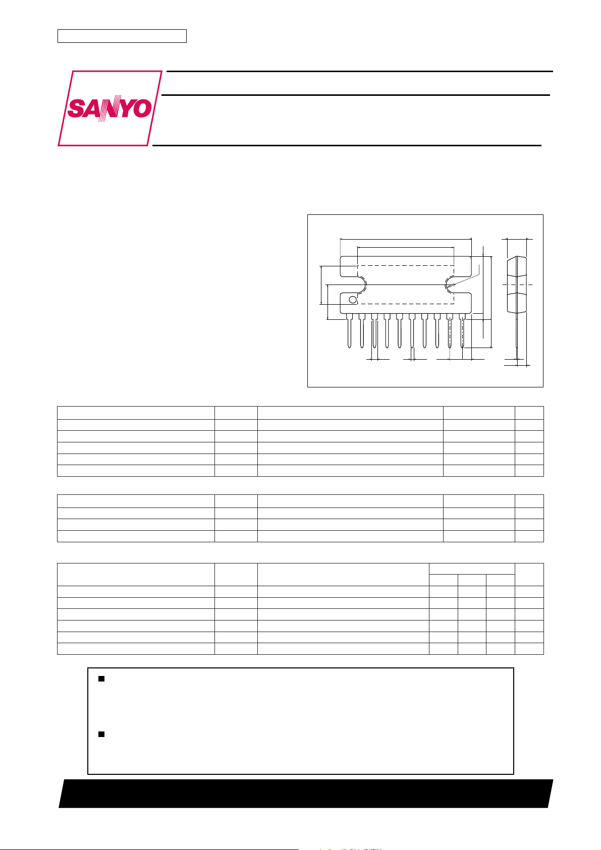
Package Dimensions
unit:mm
3024A-SIP10H
[LA4270]
27.0
20.0
strap capacitor requierd).
• Low pop noise at the time of power switch ON/OFF.
• High ripple rejection (58dB typ).
• Wide supply voltage range (10V to 32V).
• On-chip protector against abnormality (thermal shutdown,
8.4
7.0
R1.7
11.8
13.2max
overvoltage).
6.0
1.0min
2.54
101
2.07
SANYO : SIP10H
Specifications
1.4
0.5
Absolute Maximum Ratings at Ta = 25˚C
retemaraPlobmySsnoitidnoCsgnitaRtinU
egatlovylppusmumixaMV
tnerructuptuomumixaMI
noitapissidrewopelbawollAxamdP.hpargaT–dPeeS.knistaehhtiW 02W
erutarepmetgnitarepOrpoT 57+ot02–
erutarepmetegarotSgtsT 051+ot04–
xam 53V
CC
kaep 5.3V
O
Operating Conditions at Ta = 25˚C
retemaraPlobmySsnoitidnoCsgnitaRtinU
egatlovylppusdednemmoceRV
egnaregatlovgnitarepOV
ecnatsiserdaoldednemmoceRR
CC
po 23ot01V
CC
L
Operating Characteristics at Ta = 25˚C, VCC=25V, RL=8Ω, f=1kHz, Rg=600Ω, See specified test circuit
retemaraPlobmySsnoitidnoC
tnerructnecseiuQI
niagegatloVGV830424Bd
rewoptuptuOP
noitrotsidcinomrahlatoTDHTPOW2=1.08.0%
egatlovesiontuptuOV
noitcejerelppiRRRVSk01=gR Ω f,
OCC
O
ON
%1=DHT0.50.6W
k01=gR Ω zHk02otzH02=WB,52.00.1Vm
V,zH001=
R
mBd0=5485Bd
R
nimpytxam
sgnitaR
525409Am
Continued on next page
4.0
0.4
2.0
˚C
˚C
52V
Ω
8
tinU
21500TH (KT)/40194HK/3210MO/8026KI/6126AT/6245KI, TS No.1724–1/9
LA4270
Continued from preceding page.
retemaraPlobmySsnoitidnoC
klatssorCTCk01=gR Ω 5406Bd
ecnalablennahC
∆ GV
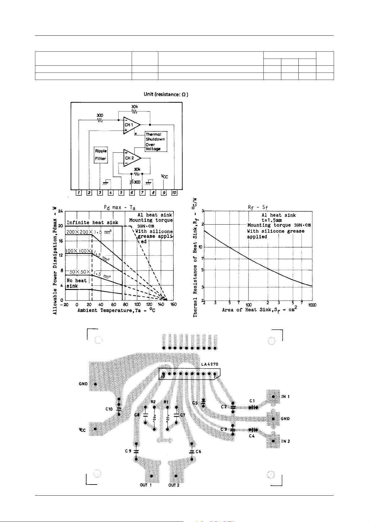
Equivalent Circuit Block Diagram and Pin Assignment
nimpytxam
sgnitaR
tinU
5.1Bd
Sample Printed Circuit Pattern
No.1724–2/9
LA4270
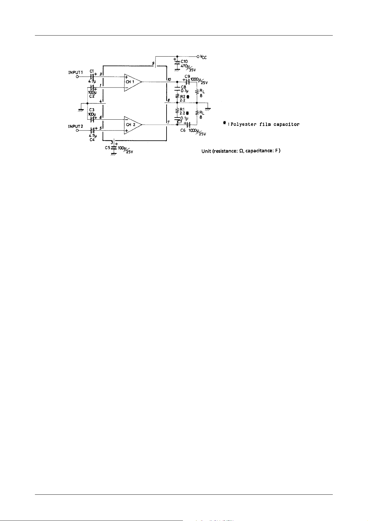
Sample Application Circuit 1 : Dual-channel use (specified Test Circuit)
Description of External Parts
C1, C4 : Input capacitors
(4.7µF) Since the DC potential of the input pins is not 0, the two capacitors cannot be omitted. Decreasing the
capacitor value extremely causes the frequency response to lower at low frequencies.
C2, C3 : Feedback capacitors
(100µF) Decreasing the capacitor value causes the frequency response to lo wer at lo w frequencies. Increasing
the capacitor value makes the starting time later.
C5 : Ripple filter capacitor
(100µF/25V) Decreasing the capacitor value provides less ripple rejection. Decreasing the capacitor value also
makes the starting time earlier.
C6, C9 : Output capacitors
(1000µF/25V) Decreasing the capacitor value provides less power at low frequencies.
C7, C8 : Oscillation blocking capacitors
(0.1µF polyester Decreasing the capacitor value causes oscillation to be liable to occur. It is recommended to use
film capacitors) polyester film capacitors which are excellent in high frequency response, temperature c haracteristic.
The use of electrolytic capacitors or ceramic capacitors may cause oscillation to occur at low temperatures.
C10 : Power capacitor
(470µF/35V) Decreasing the capacitor value causes ripple to be liable to occur. If the distance between the IC and
this capacitor is made long or this capacitor is removed, oscillation may occur.
R1, R2 : Resistors connected in series with oscillation blocking capacitors
(2.2Ω) Used to prevent phase shift attributable to the oscillation blocking capacitors so that oscillation is
hard to occur. Increasing or decreasing the resistor value causes oscillation to be liable to occur. The
optimum value must be used.
No.1724–3/9
 Loading...