

Page 1
Any and all SANYO products described or contained herein do not have specifications that can handle
applications that require extremely high levels of reliability, such as life-support systems, aircraft’s
control systems, or other applications whose failure can be reasonably expected to result in serious
physical and/or material damage. Consult with your SANYO representative nearest you before using
any SANYO products described or contained herein in such applications.
SANYO assumes no responsibility for equipment failures that result from using products at values that
exceed, even momentarily, rated values (such as maximum ratings, operating condition ranges,or other
parameters) listed in products specifications of any and all SANYO products described or contained
herein.
Monolithic Linear IC
3.5W Monaural Power Amplifier
Ordering number:ENN1463C
LA4265
SANYO Electric Co.,Ltd. Semiconductor Company
TOKYO OFFICE Tokyo Bldg., 1-10, 1 Chome, Ueno, Taito-ku, TOKYO, 110-8534 JAPAN
Features
• Minimum number of external parts requierd (No input
capacitor, bootstrap capacitor requierd).
• High output : 3.5W typ (VCC=16V, RL=8Ω, THD=10%).
• Soft clip, causing little harmonic disturbance to radios.
• Small pop noise at the time of power switch ON/OFF.
• Built-in protector against abnormal modes (Thermal shut-
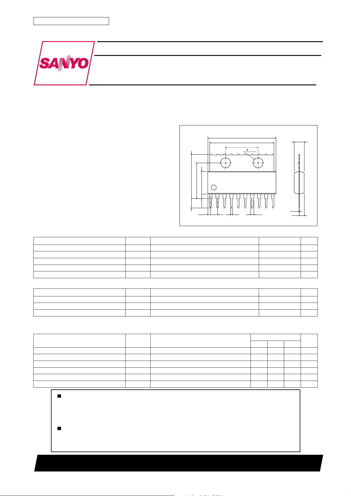
Package Dimensions
unit:mm
3018A-SIP10FD
[LA4265]
25.5
24.0
12.0
3.6
down, overvoltage)
16.7max
13.5
8.4
3.5
Specifications
1.32
1.6min
2.54
0.5
1.3
101
SANYO : SIP10FD
Absolute Maximum Ratings at Ta = 25˚C
retemaraPlobmySsnoitidnoCsgnitaRtinU
egatlovylppusmumixaMV
tnerructuptuomumixaMI
noitapissidrewopelbawollAxamdP001htiW × 021 × mm5.1
erutarepmetgnitarepOrpoT 57+ot02–
erutarepmetegarotSgtsT 051+ot04–
xam 52V
CC
kaep 2A
o
3
knistaehlA5.7W
Operating Conditions at Ta = 25˚C
retemaraPlobmySsnoitidnoCsgnitaRtinU
egatlovylppusdednemmoceRV
ecnatsiserdaoldednemmoceRR
egnaregatlovylppusgnitarepOV
CC
L
CC
Operating Characteristics at Ta = 25˚C, VCC=16V, RL=8Ω, f=1kHz, Rg=600Ω, See specified test circuit
(based on sample application circuit).
retemaraPlobmySsnoitidnoC
tnerructnecseiuQI
niagegatloVGV840525Bd
rewoptuptuOP
noitrotsidcinomrahlatoTDHTPOW5.0=3.00.1%
egatlovesiontuptuOV
noitcejerelppiRRRVSf,0=gR
OCC
O
ON
%01=DHT0.35.3W
k01=gR Ω zHk02otzH02=FPB,56.05.1Vm
V,zH001=
R
V5.0=0405Bd
R
nimpytxam
sgnitaR
5305Am
3.6
0.45
1.6
˚C
˚C
61V
Ω
8
42ot9V
tinU
21500TH (KT)/33194HO/0237KI/8064KI/4034KI, TS No.1463–1/8
Page 2
LA4265
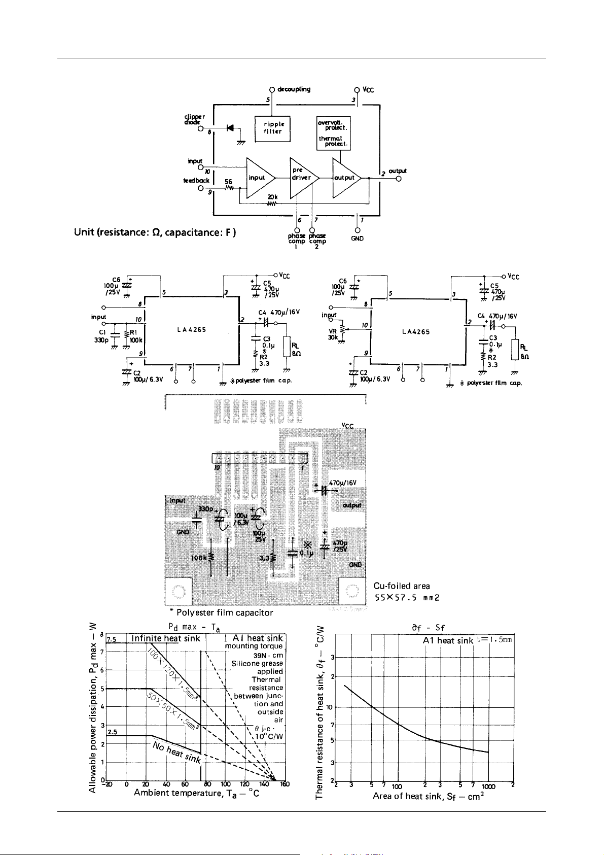
Equivalent Circuit Block Diagram
Sample Application Circuit 1 Sampl Application Circuit 2
(Recommended circuit) (Circuit with minimum number of external parts)
Sample Printed
Circuit Pattern
No.1463–2/8
Page 3

LA4265
Description of External Parts
C1 (330pF) : Input short capacitor
Reduces the high frequency noise when the input impedance is increased. Not required when the input
impedance is decreased.
C2 (100µF) : Feedback capacitor
Decreasing the capacitance value lowers the low frequency response. Increasing the capacitance value
makes the starting time later.
C3 (0.1µF : Oscillation blocking capacitor
polyester film Decreasing the capacitance value causes oscillation to occur easily. Use a polyester film capacitor that is
capacitor) good in high frequency response and temperature characteristic. The use of an electrolytic capacitor may
cause oscillation to occur at low temperatures.
C4 (470µF) : Output capacitor
Decreasing the capacitance value causes insufficient power at low frequencies.
C5 (470µF) : Power capacitor
Decreasing the capacitance value causes ripple to occur easily. Locating at a distance from the IC or
removing this capacitor may cause oscillation to occur.
C6 (100µF) : Ripple filter capacitor
Decreasing the capacitance value excessiv ely or remo ving this capacitor causes ripple to occur. Howe v er,
increasing the capacitance value does not always cause ripple to be reduced. Decreasing the capacitance
value makes the starting time earlier.
R1 (100kΩ) : Input bias resistor
Determines the bias (bias of zero potential) to be applied to the input pin and the input impedance. Not
required if a variable resistor is also used as this resistor.
R2 (3.3Ω) : Resistor connected in series with oscillation blocking capacitor
Prevents phase shift attributable to the oscillation blocking capacitor so that oscillation is hard to occur.
Note for Changing Voltage Gain
The voltage gain can be reduced by adding an external resistor (RNF) in series with the feedback capacitor. (See VG · R
characteristic curve). Howe v er , it should be noted that v arious character istics are also changed (THD-VG, VNO-VG, VroVG). The voltage gain must not be reduced to be less than 30dB. Since the frequenc y response is extended and oscillation
is liable to occur when the voltage gain is reduced, high-cut must be made as required. (High-cut is made by connecting
a capacitor of approximately 30pF across pins (6) and (7).)
External Muting
If external muting is required, make the circuit as shown on next pag e. In this case, the pop noise is similar to that which
occurs at the time of power switch ON/OFF. If the value of the series resistor is decreased, more pop noise is heard at the
time of attack ; if increased, muting is hard to work.
Measure against Fold-back of Output Waveform
Since the input pin is zero-biased, the circuit may be saturated at an overinput, causing a part of the output wa veform to
be folded back (e. g. when the peak input voltage exceeds 600mV). In such a case, the fold-back of the wav eform can be
prevented by using the built-in diode (also can be prevented by using an external diode). When the b uilt-in diode is used,
a resistor must be connected in series with the input pin to cause the diode to conduct no overcurrent (10mA or less).
NF
No.1463–3/8
Page 4

Fold-back Output Waveform
LA4265
No.1463–4/8
Page 5

LA4265
No.1463–5/8
Page 6

LA4265
No.1463–6/8
Page 7

LA4265
Proper Cares in Using IC
• Maximum ratings
If the IC is used in the vicinity of the maximum ratings, even a slight var iation in conditions may cause the maximum
ratings to be exceeded, thereby leading to breakdown. Allow an ample mar gin of variation for supply voltage, etc. and
use the IC in the range where the maximum ratings are not exceeded.
• Pin-to-pin short
If power is applied when the space between pins is shorted, breakdown or deterioration may occur. When mounting the
IC on the board or applying power, make sure that the space between pins is not shorted with solder, etc.
• When used in radio applications
When using in radios, allow a sufficient space between IC and bar antenna.
No.1463–7/8
Page 8

LA4265
• Printed circuit pattern
When designing the printed circuit pattern, make the power supply, output, and ground lines thick and short and
arrange the pattern and parts so that no feedback loop is formed between input and output. Place power capacitor C5,
oscillation blocking capacitor C3 as close to IC pins as possible to prevent oscillation from occurring. Refer to the
sample printed circuit pattern.
• Some plug jacks to be used for connecting to the external speaker can have the both poles short-circuited once when
connecting. In this case, the load is short-circuited, which may break down the IC.
Specifications of any and all SANYO products described or contained herein stipulate the performance,
characteristics, and functions of the described products in the independent state, and are not guarantees
of the performance, characteristics, and functions of the described products as mounted in the customer's
products or equipment. To verify symptoms and states that cannot be evaluated in an independent device,
the customer should always evaluate and test devices mounted in the customer's products or equipment.
SANYO Electric Co., Ltd. strives to supply high-quality high-reliability products. However, any and all
semiconductor products fail with some probability. It is possible that these probabilistic failures could
give rise to accidents or events that could endanger human lives, that could give rise to smoke or fire,
or that could cause damage to other property. When designing equipment, adopt safety measures so
that these kinds of accidents or events cannot occur. Such measures include but are not limited to protective
circuits and error prevention circuits for safe design, redundant design, and structural design.
In the event that any or all SANYO products(including technical data,services) described or
contained herein are controlled under any of applicable local export control laws and regulations,
such products must not be exported without obtaining the export license from the authorities
concerned in accordance with the above law.
No part of this publication may be reproduced or transmitted in any form or by any means, electronic or
mechanical, including photocopying and recording, or any information storage or retrieval system,
or otherwise, without the prior written permission of SANYO Electric Co. , Ltd.
Any and all information described or contained herein are subject to change without notice due to
product/technology improvement, etc. When designing equipment, refer to the "Delivery Specification"
for the SANYO product that you intend to use.
Information (including circuit diagrams and circuit parameters) herein is for example only ; it is not
guaranteed for volume production. SANYO believes information herein is accurate and reliable, but
no guarantees are made or implied regarding its use or any infringements of intellectual property rights
or other rights of third parties.
This catalog provides information as of February, 2000. Specifications and information herein are subject
to change without notice.
PS No.1463–8/8
 Loading...