

SANYO LA4182 Datasheet
Ordering number: EN742G
Monolithic Linear IC
LA4182
2.3 W 2-Channel AF Power Amplifier
Features
.
Built-in 2 channels enabling use in stereo and bridge
amplifier applications.
.
High output: 2.3 W/channel, VCC=9V,RL=4Ω, and
4.7 W/bridge, R
.
Minimum number of external parts required : 9 pcs. min.
(Stereo/bridge).
.
Small pop noise at the time of power supply ON/OFF due to
built-in muting circuit.
.
Good ripple rejection ratio due to built-in ripple filter.
.
Soft tone at the time of output saturation.
.
Good channel separation.
.
Voltage gain fixed at 45 dB (Bridge: 51 dB). Variable
voltage gain available with external resistor added.
.
Easy to design radiator fin.
=8Ω.
L
Specifications
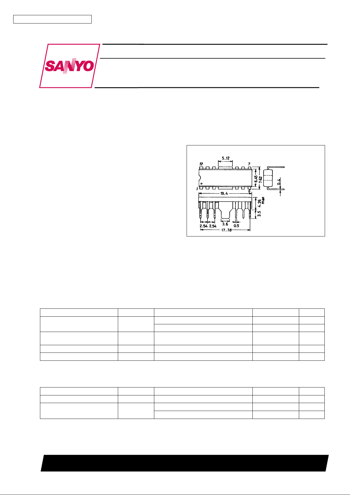
Package Dimensions
unit : mm
3022A-DIP12F
[LA4182]
SANYO : DIP12F
Note) In general applications, heat generated in this package
can be radiated through the Cu-foiled area of the printed
circuit board, but since power dissipation Pd may be
increased depending on the supply voltage and load
conditions, it is recommended to use a fin additionally.
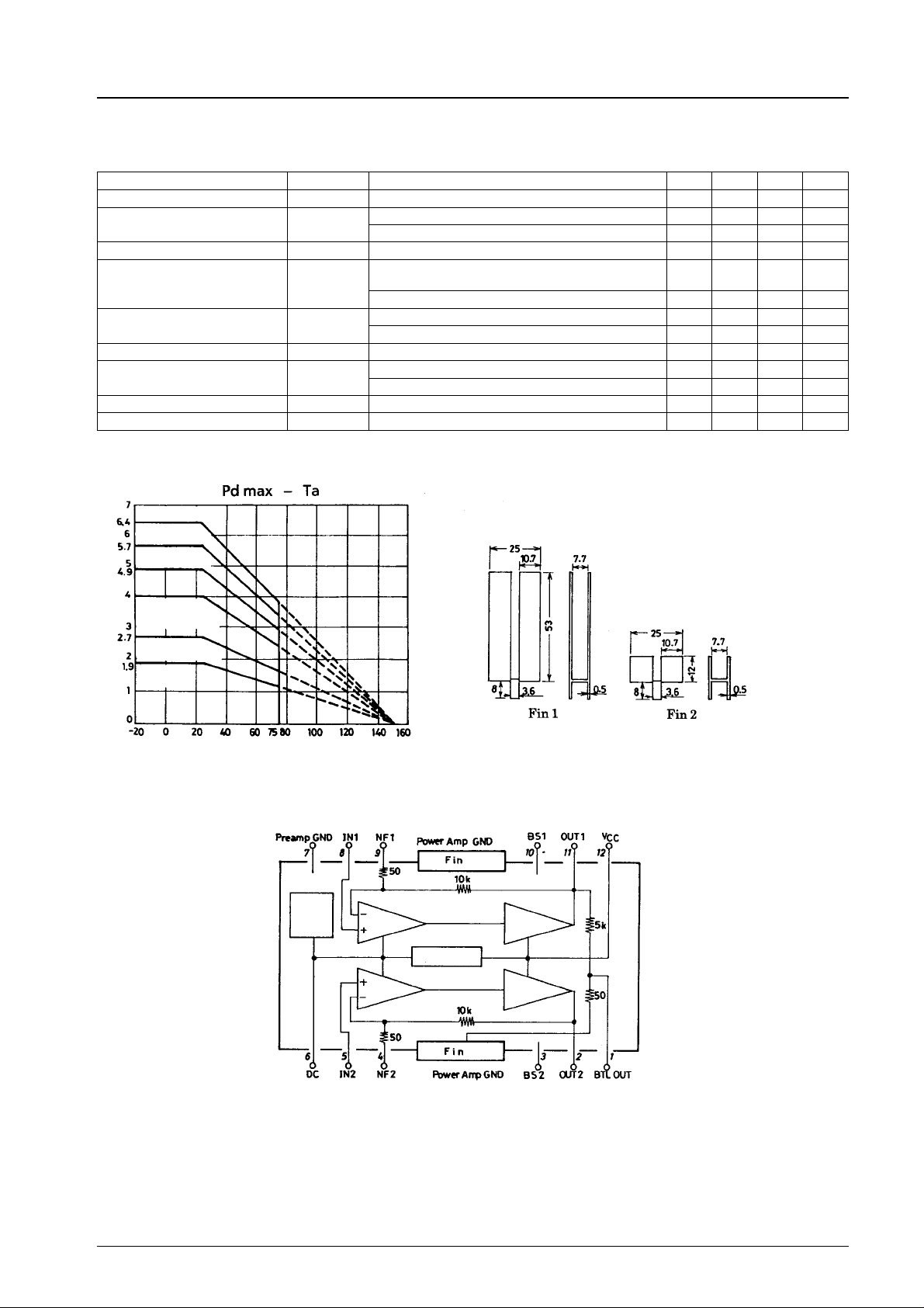
Maximum Ratings at Ta = 25°C
Parameter Symbol Conditions Ratings Unit
Maximum supply voltage V
Allowable power dissipation Pd max
Operating temperature Topr −20 to +75 °C
Storage temperature Tstg −55 to +150 °C
CC
max
With signal 11 V
Quiescent 15 V
With printed circuit board
(Refer to Pd-Ta characteristics)
4W
Recommended Operating Conditions at Ta = 25°C
Parameter Symbol Conditions Ratings Unit
Supply voltage V
Load resitance R
CC
L
Stereo 4 to 8 Ω
Bridge 8 Ω
9V
SANYO Electric Co.,Ltd. Semiconductor Bussiness Headquarters
TOKYO OFFICE Tokyo Bldg., 1-10, 1 Chome, Ueno, Taito-ku, TOKYO, 110 JAPAN
41596HA(II)/O207KI/2146KI/4025KI/O291KI,TS No.742-1/9
LA4182
Operating Characteristics at Ta = 25°C, VCC=9V,f=1kHz, RL=4Ω,Rg=600Ω, ( ): 8 Ω,
See specified Test Circuit.
Parameter Symbol Conditions min typ max Unit
Quiescent current I
CCO
Voltage gain VG
Voltage gain difference ∆VG Stereo ±1dB
Output power P
Total harmonic distortion THD
Input resistance r
Output noise voltage V
NO
Ripple rejection ratio R
Channel separation CHsep Rg = 10 kΩ,V
Cu plate (fin 1)
Fe plate
(fin 1)
Fe Plate
(fin 2)
Stereo Stereo 40 55 mA
Closed loop, V
= −45 dB Stereo 43 45 47 dB
IN
Closed loop, VIN = −45 dB Bridge 49 51 53 dB
THD = 10% Stereo 1.7
O
2.3
(1.3)
THD = 10% Bridge (4.7) W
= 250 mW Stereo 0.3 1.5 %
P
O
P
= 250 mW Bridge 0.5 %
O
i
21 30 kΩ
Rg = 0 Stereo 0.3 1.0 mV
Rg=10kΩ Stereo 0.5 2.0 mV
Rg=0,VR= 150 mV Stereo 40 46 dB
r
= 0 dB Stereo 40 55 dB
O
W
Recommended
printed circuit
board only
Cu-foiled area
reduced board
IC only
Allowable power dissipation, Pd max − W
Ambient temperature, Ta − °C
Pin Assignment and Equivalent Circuit
Shock
noise
rejecter
Input
amp 1
Input
amp 2
Ripple filter
Output
amp 1
Output
amp 2
Unit (resistance: Ω)
No.742 -2/9
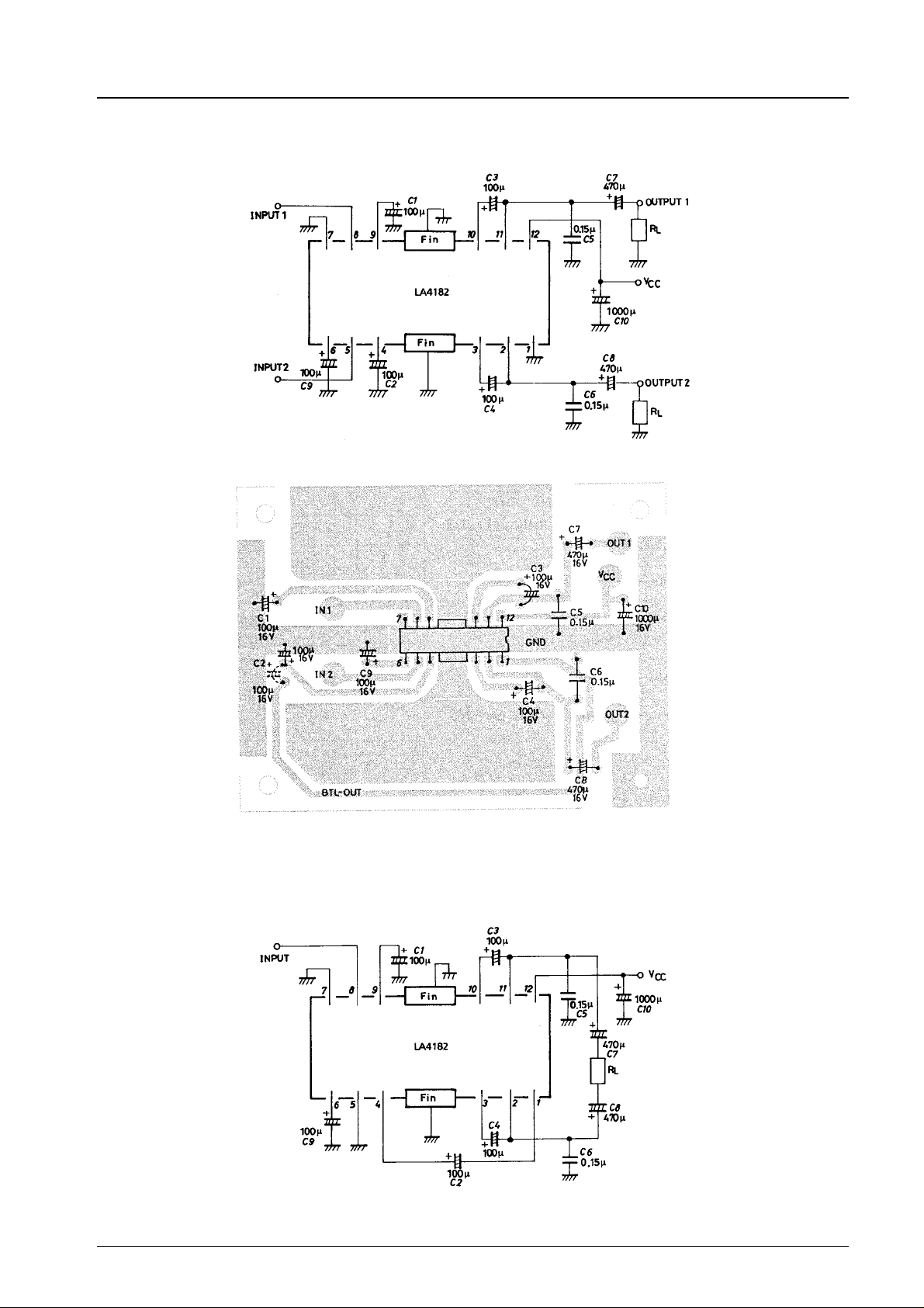
Sample Application Circuit 1 : Stereo
LA4182
(Mylar)
(Mylar)
Unit (capacitance: F)
Stereo
Bridge
Unit (capacitance: F)
Example of printed pattern (bottom view) for use in stereo, bridge amplifier applications : 60 × 80 mm
2
Sample Application Circuit 2 : Bridge
(Mylar)
(Mylar)
Unit (capacitance: F)
No.742 -3/5
 Loading...