

SANYO LA4168M Datasheet
Overview
The LA4168M is a record/playback system IC for
microcassette and compact cassette recorders. The
LA4168M is an extremely high-functionality IC that
includes a motor control governor circuit, a voice sensor
circuit that detects sounds and turns motor on or off, a
power switch control circuit that receives an electrical
signal from a photosensor and turns all of the IC function
blocks on or off, and a circuit that increases the speed of
the motor during playback.
Functions
• Microphone and playback preamplifiers
• Record amplifier
• Power amplifier (BTL, 4 Ω)
• Automatic stop circuit (power switch)
• Governor circuit
• Motor speed and high-speed switching circuit
• Microphone power supply
• LED drive circuit
• Voice sensor circuit
Features
• Includes a voice switch that can turn the governor on or
off.
• Includes a power switch circuit that can turn all the IC
function blocks on or off from a photosensor signal.
During record, the IC can automatically turn the
governor on or off according to the microphone input
level, and furthermore, the governor on/off level can be
continuously adjusted from an external control knob.
(The control used for volume adjustment during
playback.)
• Continuously variable microphone monitor level.
• Includes a drive pin for an LED that lights only when
the governor is on in record mode.
Monolithic Linear IC
Ordering number : EN5660
73097HA(OT) No. 5660-1/6
SANYO Electric Co.,Ltd. Semiconductor Bussiness Headquarters
TOKYO OFFICE Tokyo Bldg., 1-10, 1 Chome, Ueno, Taito-ku, TOKYO, 110 JAPAN
Record/Playback System for Microcassette and
Compact Cassette Recorders
LA4168M
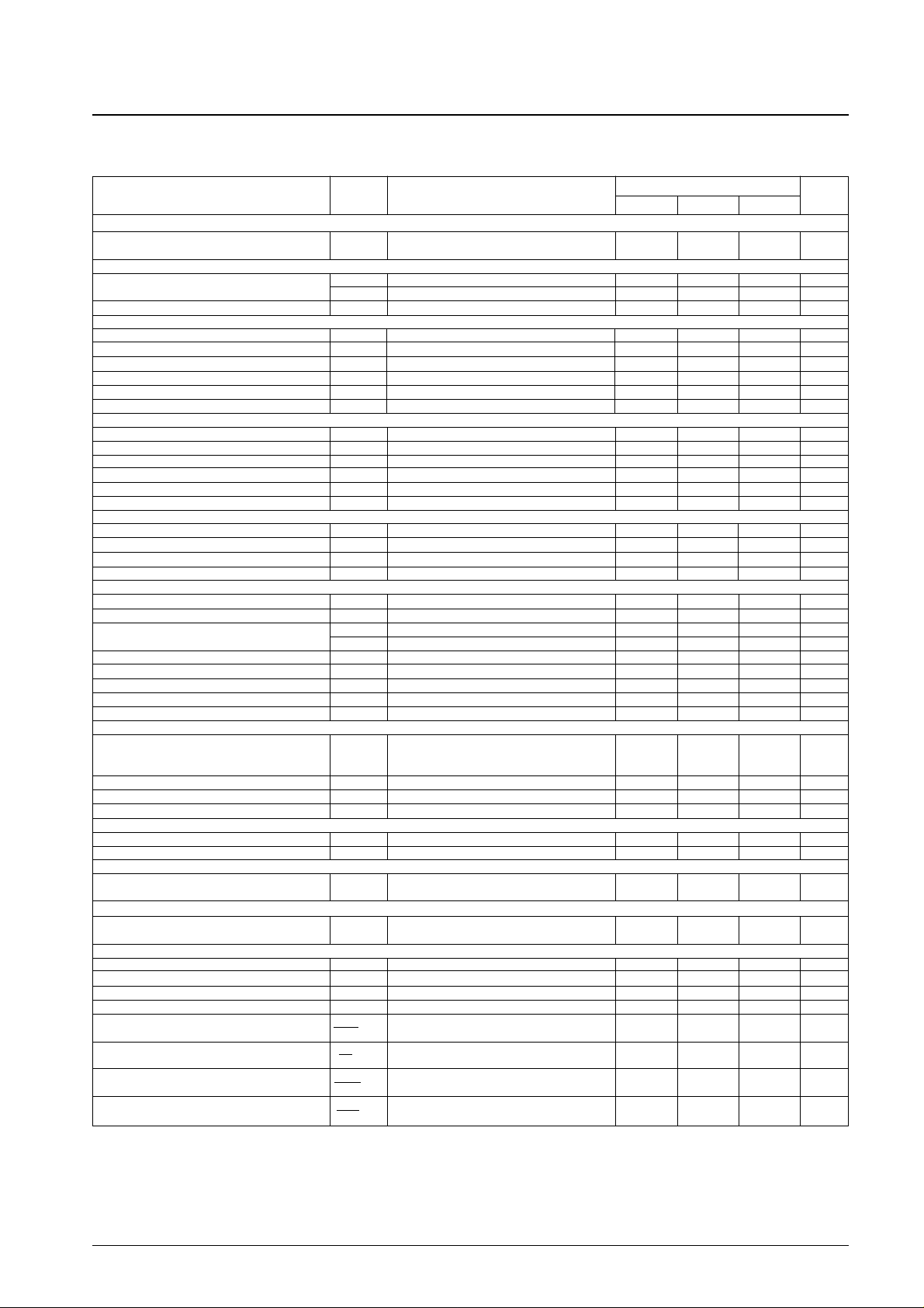
Parameter Symbol Conditions Ratings Unit
Maximum supply voltage V
CC
max 4.5 V
Allowable power dissipation Pd max 800 mW
Operating temperature Topr –10 to +50 °C
Storage temperature Tstg –55 to +150 °C
Specifications
Maximum Ratings at Ta = 25°C
Parameter Symbol Conditions Ratings Unit
Recommended supply voltage V
CC
3.0 V
Operating voltage range V
CC
op 1.8 to 3.6 V
Load resistance
(power block) R
L
pwr 4 Ω
(preamplifier block) R
L
pre 10 kΩ
Operating Conditions at Ta = 25°C
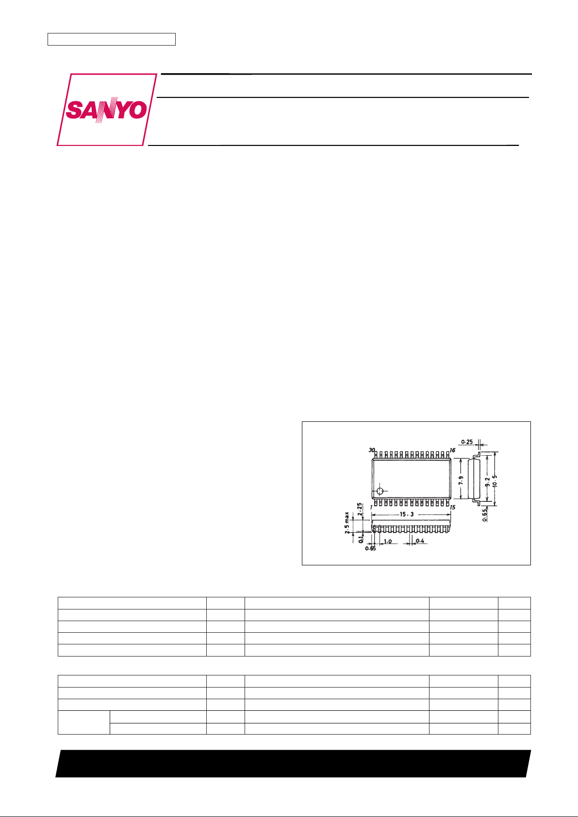
SANYO: MFP30SD
[LA4168M]
Package Dimensions
unit: mm
3073A-MFP30SD
No. 5660-2/6
LA4168M
Parameter Symbol Conditions
Ratings
Unit
min typ max
[PRE + POWER + GVN]
Standby current I
STB
With pin 9 connected to V
CC
25 170 250 µA
through a 100-kΩ resistor
[PRE + POWER]
Quiescent current
I
CC-R
REC MODE, Vi = 0 V 6 12 18 mA
I
CC-P
PLAY MODE, Vi = 0 V, VOL MIN 12 18 25 mA
Voltage gain VG
TP
PLAY MODE, VO= –5 dBm 71.5 74 76.5 dB
[EQ AMP]
Voltage gain (open loop) VG
OPCNF
= 100 µF 80 85 dB
Voltage gain (closed loop) VG
P
50 52 54 dB
Maximum output voltage V
OP
max THD = 1 % 0.5 0.75 V
Total harmonic distortion THD
PVO
= 0.3 V 0.2 0.6 %
Equivalent input noise voltage V
NIP
Rg = 2.2 kΩ, DIN audio 1.0 2.0 µV
Ripple rejection ratio R
rp
Rg = 2.2 kΩ, fR= 1 kHz filter 45 60 dB
[MIC AMP] VOL MIN, ALC OFF
Voltage gain (closed loop) VG
M
1 ALC OFF 43 45 47 dB
Maximum output voltage V
OmaxM
THD = 1 %, RL= 10 kΩ 0.5 0.75 V
Total harmonic distortion THD
MVO
= 0.3 V 0.6 1.0 %
Equivalent input noise voltage V
NIM
Rg = 3 kΩ, DIN audio 2.0 4.0 µV
Ripple rejection ratio SVRR Rg = 3 kΩ, f
R
= 1 kHz filter 40 53 dB
Input resistance R
IM
24 32 40 kΩ
[MIC + REC] VOL MIN
Voltage gain (closed loop) VG
RT
ALC OFF 63.5 65.5 67.5 dB
Maximum output voltage V
OmaxR
THD = 5 % 0.6 1.0 V
Output noise voltage V
NORT
MIC Input, Rg = 3 kΩ, DIN audio 3.5 8.0 mV
Ripple rejection ratio R
rRT
Rg = 3 kΩ, fR= 1 kHz , 1 kHz filter 20 32 dB
[POWER AMP]
Voltage gain (closed loop) VG
BTL
BTL ON, VO= –10 dBm 21.5 24 26.5 dB
Voltage gain (closed loop) VG
SIN
Single, VO= –10 dBm 20.5 23 25.5 dB
Output power
P
OBTL
THD = 10 %, BTL ON 200 350 mW
P
OSIN
THD = 10 %, Single 50 120 mW
Total harmonic distortion THD
BTL
BTL ON, VO= 0.25 V 0.1 0.8 2 %
Output noise voltage V
NOBTL
BTL ON, Rg = 0 kΩ 20 50 µV
Ripple rejection ratio R
rBTL
BTL ON, Rg = 0 kΩ, fR= 1 kHz , 1 kHz filter 50 70 dB
Output DC offset V
DCOFF
BTL ON, Rg = 0 kΩ 0 10 50 mV
Input resistance R
INBTL
21 30 39 kΩ
[ALC]
The input level width from the point the ALC
ALC width ALC
W
circuit operates to the point the harmonic 40 67 dB
distortion reaches 5%
ALC harmonic distortion ALC
THD
Vim = –40 dBm 1.0 2.0 %
ALC output ALC V
O
Vim = –40 dBm 0.33 0.43 0.53 V
ALC start input ALC V
IN
Vim = –40 dBm –79 –74 –69 dBm
[Voice Sensor (VOX)]
Operation start input voltage V
OP min
VOLUME (10 kΩ) max –90 –85 –80 dBm
Input hysteresis V
O HL
3 6 9 dB
[Auto-Stop]
Operation voltage V
I ATS
The pin 9 voltage at the point the auto-stop
0.65 0.7 V
circuit operates
[LED]
LED drive current I
LED
The input current when shorted
8 15 22 mA
through a 300-Ω resistor
[GVN]
Reference voltage Vref Im = 100 mA 1.1 1.25 1.4 V
Current division ratio K Im = 50 – 100 mA 45 50 55
Residual voltage Vsat V
REF
= CONT, Im = 200mA 0.1 0.2 0.5 V
The CONT pin voltage in speed up mode Vcont 0.35 0.41 0.47 V
Reference voltage/voltage characteristics
∆Vref
/∆V
CCVCC
= 1.8 to 4.5 V, Im = 100 mA 0 0.2 0.6 %/V
Vref
Current division ratio/voltage characteristics
∆K
/∆V
CCVCC
= 2.0 to 4.5 V, Im = 50 – 100 mA 0 0.3 0.7 %/V
K
Reference voltage/current characteristics
∆Vref
/∆Im
Im = 50 – 200 mA 0 0.002 0.03 %/mA
Vref
Current division ratio/current characteristics
∆K
/∆Im
Im = 50 – 100 mA to 150 – 200 mA –0.07 0.03 +0.07 %/mA
Vref
Operating Characteristics at Ta = 25°C, VCC= 3.0 V, RL= 4 Ω (power amplifier), RL= 10 kΩ (preamplifier),
f = 1 kHz, 0 dBm = 0.775 V
 Loading...