

Page 1
Ordering number : ENN4036C
42000TN (OT)/D2599TH (OT)/O282TS / 9121YO No. 4036-1/20
0.25
15.3
1
15
30
16
0.65
0.4
1.0
2.5max
2.250.1
0.65
7.9
9.2
10.5
SANYO: MFP30SD
[LA4167M]
LA4167M
SANYO Electric Co.,Ltd. Semiconductor Company
TOKYO OFFICE Tokyo Bldg., 1-10, 1 Chome, Ueno, Taito-ku, TOKYO, 110-8534 JAPAN
1-channel Record/Playback System
for Microcassette and Compact Cassette Recorders
Monolithic Linear IC
Any and all SANYO products described or contained herein do not have specifications that can handle
applications that require extremely high levels of reliability, such as life-support systems, aircraft’s
control systems, or other applications whose failure can be reasonably expected to result in serious
physical and/or material damage. Consult with your SANYO representative nearest you before using
any SANYO products described or contained herein in such applications.
SANYO assumes no responsibility for equipment failures that result from using products at values that
exceed, even momentarily, rated values (such as maximum ratings, operating condition ranges, or other
parameters) listed in products specifications of any and all SANYO products described or contained
herein.
Overview
The LA4167M is a record/playback system IC
supporting microcassette and compact cassette recorders.
This is a high-performance IC that has on-chip a
governor circuit for motor control, a voice sensor circuit
that detects sounds and switches the motor on and off,
and a cue-tone circuit for instantly finding the desired
segment to play back.
Functions
• Microphone and playback preamps
• Record amplifier
• Power amplifier (BTL 4 Ω — single power during
recording)
• Cue-tone oscillator and current amplifier (15 Hz typ.
sine wave)
• Governor circuit
• Microphone power supply
• LED drive
Features
• Can switch between recording and playback with a
single mechanical switch.
• Pause switch can switch the governor on and off.
• Cue-tone switch can record specified oscillator output
(sine wave) during recording.
• The governor can automatically be switched on or off
according to the mike input level during recording, and
the on/off level for the governor can be varied
continuously by the external volume control (used to
adjust volume during playback).
• Mike monitor level is continuously variable.
• LED pin for turning off the LED only when cue-tone is
on.
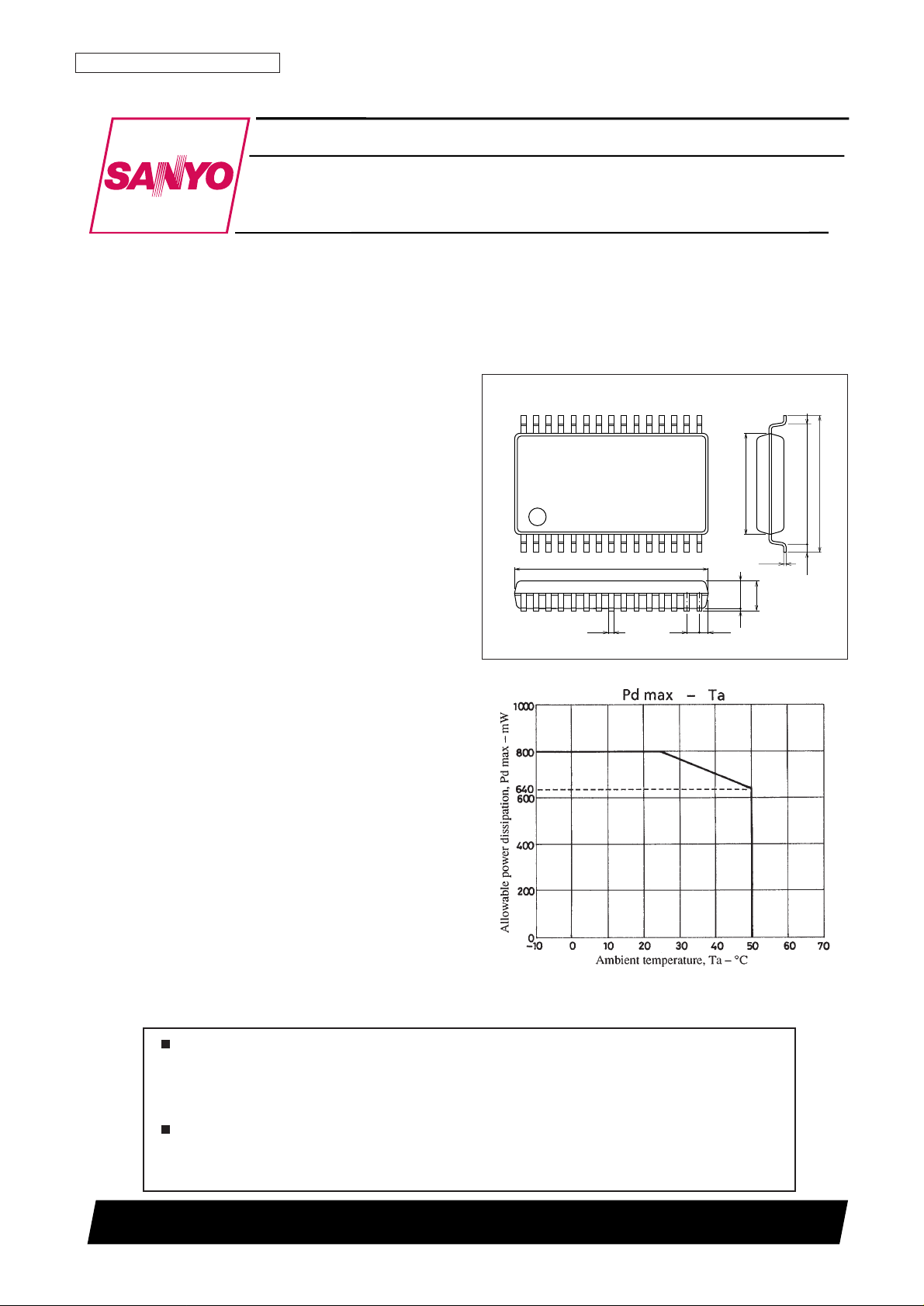
Package Dimensions
unit: mm
3073A-MFP30SD
Page 2
LA4167M
No. 4036-2/20
Parameter Symbol Conditions Ratings Unit
Maximum supply voltage V
CC
max 4.5 V
Allowable power dissipation Pd max 800 mW
Operating temperature Topg –10 to +50 °C
Storage temperature Tstg –55 to +150 °C
Specifications
Maximum Ratings at Ta = 25°C
Operating Conditions at Ta = 25°C
Parameter Symbol Conditions Ratings Unit
Recommended supply voltage V
CC
3.0 V
Power supply voltage operating range V
CC
op 1.8 to 3.6 V
Resistance load (power) R
L
pwr 4 Ω
Resistance load (preamp) R
L
pre 10 kΩ
Operation Characteristics at Ta = 25°C, VCC= 3.0 V, RL= 4Ω (power), RL= 10 kΩ (preamp), f = 1 kHz,
0 dBm = 0.775 V PLAY mode during BTL, REC mode during single
Parameter Symbol Conditions
Ratings
Unit
min typ max
[Pre + Power + GVN]
Silence current
I
CC-R
REC MODE, Vi=0V 6 12 18 mA
I
CC-P
PLAY MODE, Vi=0V 12 18 25 mA
[Pre + Power]
Voltage gain VG
TP
PLAY MODE, VO=–5dBm 70 72.5 75 dB
[EQ AMP]
Voltage gain (open) VG
OPCNF
=100µF 80 85 90 dB
Voltage gain (closed) VG
P
50 52 54 dB
Maximum output voltage V
OP
max THD=1% 0.5 0.75 1.0 V
Total harmonic distortion THD
PVO
=0.3V 0.01 0.2 0.6 %
Input conversion noise voltage V
NIP
Rg=2.2kΩ, DIN AUDIO 1.0 2.0 µV
Ripple rejection Rrp Rg=2.2kΩ, f
R
=1kHz, 1kHz Filter
45 60 dB
[MIC AMP]
Voltage gain (open) VG
OMCNF
=100µF 75 80 85 dB
Voltage gain (closed) VG
MI
EQ parameter ON, 3k, 3300pF IN 44 46 48 dB
Maximum output voltage V
OMAXM
THD=1%, RL=10kΩ 0.5 0.75 1.0 V
Total harmonic distortion THD
MVO
=0.3V 0.01 0.6 1.0 %
Input conversion noise voltage V
NIM
Rg=2.2kΩ, DIN AUDIO 1.0 2.0 µV
Ripple rejection Rr
M
Rg=2.2kΩ, fR=1kHz, 1kHz Filter 45 65 dB
Input resistance R
IM
24 32 40 kΩ
[MIC + REC]
Voltage gain (closed) VG
RT
Vol min 64.5 66.5 68.5 dB
Maximum output voltage V
OMAXR
THD=5% 0.6 1.0 1.3 V
Total harmonic distortion THD
RTVO
=0.85V 0.5 1.2 3.0 %
Output noise voltage V
NORT
MIC input, Rg=2.2kΩ, DIN AUDIO 5.0 10 mV
Ripple rejection Rr
RT
38 45 dB
[POWER AMP]
Voltage gain (open) VG
BTL
BTL ON, VO=–10dBm 21.5 24 26.5 dB
Voltage gain (closed) VG
SIN
BTL OFF, VO=–10dBm 20.5 23 25.5 dB
Output power (BTL) P
OBTL
THD=10% BTL 200 350 500 mW
Output power (SIN) P
OSIN
THD=10% Single 50 120 250 mW
Total harmonic distortion THD
BTL
BTL ON, VO=0.25V 0.1 0.8 2 %
Output noise voltage V
NOBTL
BTL ON, Rg=0 10 20 50 µV
Ripple rejection Rr
BTL
BTL ON, Rg=0, fR=1kHz, 1kHz Filter 50 70 dB
Output DC offset V
DC OFF
01050mV
Input resistance R
INBTL
21 30 39 kΩ
Continued on next page.
Page 3
LA4167M
No. 4036-3/20
Continued from preceding page.
Parameter Symbol Conditions
Ratings
Unit
min typ max
[ALC]
ALC width ALC W
Input level width when output
40 50 65 dB
distortion is 5% and ALC is on
ALC distortion ALC THD Vim=–40dBm 0.1 1.5 2.5 %
ALC output ALC V
O
Vim=–40dBm 0.35 0.45 0.55 V
ALC input on ALC V
IN
–75 –70 –65 dB
[Voice sensor (VOX)]
Operation start input voltage V
OP
min VOLUME (10kΩ) max –90 –85 –80 dB
Input hysteresis V
O HL
369dB
[Oscillator]
Oscillation frequency f
OSCCOSC
=0.47µF 13.5 15 16.5 Hz
[LED]
LED drive current I
LED
REC LED 8 15 22 mA
[Governor]
Reference voltage Vref Im=100mA 1.1 1.25 1.4 V
Shunt ratio K Im=50–100mA 45 50 55
Residual voltage Vsat V
REF=VCONT
, Im=200mA 0.1 0.2 0.5 V
Reference voltage — voltage characteristics
∆Vref
/∆VCCVCC=1.8 to 4.5V, Im=100mA 0 0.2 0.6 %/V
Vref
Shunt voltage ratio — voltage characteristics
∆K
/∆VCCVCC=2.0 to 4.5V, Im=50–100mA
0 0.3 0.7 %/V
K
Reference voltage — current characteristics
∆Vref
/∆Im Im=50–200mA 0 0.002 0.03 %/mA
Vref
Shunt voltage ratio — current characteristics
∆K
/∆Im Im=50–100mA to 150–200mA –0.07 +0.03 +0.07 %/mA
K
Pin Array and Block Diagram
Page 4
LA4167M
No. 4036-4/20
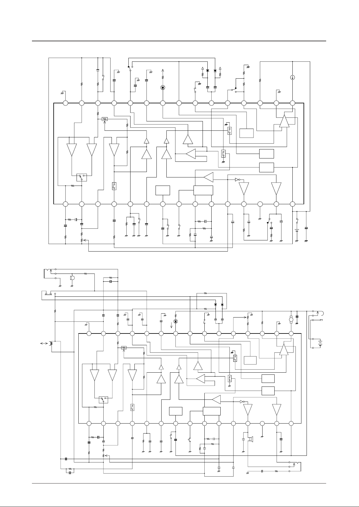
Test Circuit
1
27k
Ω
100
Ω
RX
300k
Ω
RX
2.2k
Ω
RX
2k
Ω
RX
20k
Ω
30k
Ω
470k
Ω
10k
Ω
2.2k
Ω
4700pF
1
µ
F
33
µ
F
K1
4.7
µ
F
22
µ
F
0.47
µ
F
1
µ
F
1
µ
F
0.033
µ
F
0.082
µ
F
10
µ
F
220
µ
F
3300pF
1000pF
1
µ
F
22
µ
F
+
+
+
+
++
+
+
+
PRE
NF
PRE
GND
EQ
IN
MIC
IN
V
REF
OUT
MIC
V
CC
R.F
OUT
LED
DRIVE
LED
Play
R/P
SW
PAUSE
R/P
MUTE
GVN
CONT
GVN
V
REF
VS
Im
GVN
GND
GVN
OUT
PRE
OUT
REC
IN
REC
OUT
ALC
CONT
VOX
CONT
VOX
DELAY
Cue
Tone
ON/OFF
Cue
Tone
OSC
Cue
Tone
OUT
PWR
IN
PWR
OUT1
PWR
GND
PWR
OUT2
V
CC
10k
Ω
1M
Ω
+
2
K2K8K3
K4
VCC
SW
ALC VOX
VOX Cue-Tone
R.F
R/P
GVN
POWER
V
REF
RECMICEQ
51.5dB
+
–
++
–
+
–
–
MIC
V
CC
1
PAUSE
A12755
+
4
Ω
4
Ω
K5
Vref
V
CC
(a)
100
µ
F
+
Vref
K6
20k
Ω
100
Ω
10k
Ω
50k
Ω
30k
Ω
30k
Ω
300
Ω
3k
Ω
2.2k
Ω
500k
Ω
0.47µF
23456789101112131415
161718192021222324252627282930
0.082
µ
F
470
µ
F
+
220
µ
F
3.0V
K7
REC
Sample Application Circuit
1
R3
27k
Ω
R2
100
Ω
RX
300k
Ω
RX
2.2k
Ω
RX
2k
Ω
RX
20k
Ω
30k
Ω
R5
470k
Ω
R4
10k
Ω
2.2k
Ω
C4
4700pF
C5
1
µ
F
C7
33
µ
F
C8
4.7
µ
F
C9
22
µ
F
C10
0.47
µ
F
C17
220
µ
F
C19
1
µ
F
C20
1
µ
F
C14
0.082
µ
F
C15
1µF
R9
C15
0.082
µ
F
C26
0.033µF
C21
10
µ
F
C22
220
µ
F
C23
100
µ
F
C24
4700pF
C25
6800pF
C12
1000pF
C13
0.033
µ
F
C6
1
µ
F
C3
22
µ
F
+
+
+
+
+
++
+
++
+
+
PRE
NF
PRE
GND
EQ
IN
MIC
IN
V
REF
OUT
MIC
V
CC
R.F
OUT
LED
DRIVE
LED
MIC.JK
PLAY
R/P.HEAD
REC
C.M
EAR.PH.JK
R/P
SW
PAUSE
R/P
MUTE
GVN
CONT
GVN
V
REF
VS
GVN
GND
GVN
OUT
PRE
OUT
REC
IN
REC
OUT
ALC
CONT
VOX
CONT
VOX
DELAY
Cue
Tone
ON/OFF
Cue
Tone
OSC
Cue
Tone
OUT
PWR
IN
PWR
OUT1
PWR
GND
PWR
OUT2
V
CC
R6
1M
Ω
+
2
ALC VOX
VOX Cue-Tone
R.F
R/P
GVN
POWER
V
REF
RECMICEQ
51.5dB
+
–
++
–
+
–
–
MIC
V
CC
1
PAUSE
A12756
R7
20k
Ω
R17
12k
Ω
R14
30k
Ω
R13
30k
Ω
R18
6.8k
Ω
R10
100
Ω
R12
10k
Ω
R15
300
Ω
R16
3k
Ω
R19
6.8k
Ω
R11
51k
Ω
R1
10k
Ω
R8
500k
Ω
C11
0.47µF
C1
47µF
C2
+
23456789101112131415
161718192021222324252627282930
Page 5
LA4167M
No. 4036-5/20
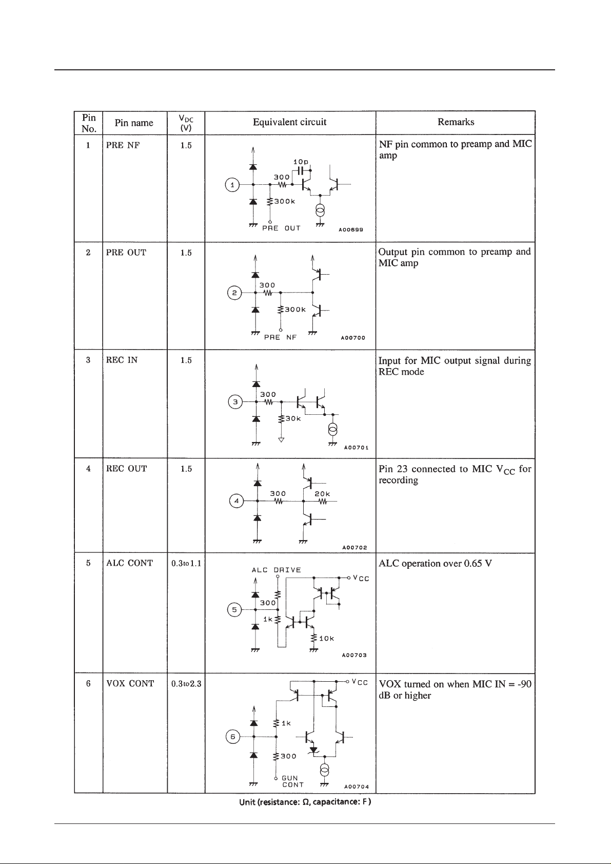
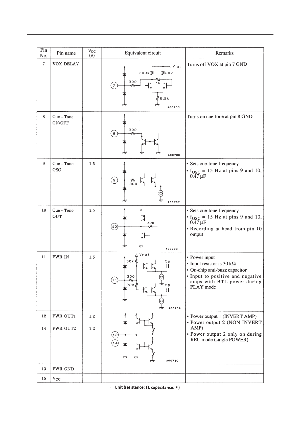
Pin Assignments and Equivalent Circuits
[VCC=3.0V]
Continued on next page.
Page 6
LA4167M
No. 4036-6/20
Continued from preceding page.
Continued on next page.
Page 7

LA4167M
No. 4036-7/20
Continued from preceding page.
[VCC=3.0V, Im=100mA, RT=100Ω]
Page 8

LA4167M
No. 4036-8/20
[VCC=3.0V, LED Load 300Ω]
Page 9

LA4167M
No. 4036-9/20
[VCC=3.0V]
Page 10

LA4167M
No. 4036-10/20
Description of Externally Mounted Parts
Continued on next page.
Page 11

LA4167M
No. 4036-11/20
IC Usage Cautions and Explanation of Operation
(1) Playback preamp and power amp voltage gain distribution during playback
• The voltage gain of the preamp can be adjusted by resistor R2, connected externally. In this case, be aware that
varying the voltage gain causes the voltage gain for the playback preamp and the mike amp to be each varied
simultaneously.
Continued from preceding page.
Page 12

LA4167M
No. 4036-12/20
(2) Mike amp, REC amp, and power amp voltage gain distribution during recording
• Be aware that during recording, the power amp is not BTL, and there is single operation for only power amp 2.
(3) VOX circuit (VOX equivalent circuit)
• VOX on time can be adjusted by varying C8 at pin 6. Increasing the capacitance delays attack time, and reducing
capacitances hastens it (VOX on = Approx. 40 ms when C8 = 4.7 µF and C9 = 22 µF).
• VOX off time can be adjusted by varying C9 at pin 7 (VOX off = Approx. 4s when C8 = 4.7 µF and C9 = 22 µF).
• To continue VOX circuit operation when MIC input is below the specified level, increase the capacitance of the
capacitor between pin 7 and V
CC
.
• To keep the governor circuit on after the VOX circuit is switched off, turn on the switch and ground pin 7 in the
equivalent circuit shown above.
• Only a capacitor is mounted between pin 6 and ground. A resistor is not mounted because when the VOX circuit
is turned on, a minute charging current is present at pin 6, and the resistance would bypass this minute current,
causing a delay in operation and, in the worst case, failure of the VOX circuit to operate.
• The VOX circuit has a hysteresis width of approximately 6 dB. But as shown in the figure above, the VOX
circuit is switched on when the voltage at pin 6 is over approximately 1.3 V, and is switched off when voltage is
below approximately 0.7 V. The bias to keep the VOX circuit on at this time must be an average or smooth
voltage over approximately 0.75 V.
Page 13

LA4167M
No. 4036-13/20
(4) Cue-tone (externally mounted cue-tone circuit)
• Cue-tone begins to operate at the pin 8 ground, as shown in the figure above. The LED goes out at this time.
• Capacitors C10 and C11 for cue-tone operation must be of high quality and of identical precision.
• Capacitors C10 and C11 can be varied to change the cue-tone frequency. Increasing the capacitance of C10 and
C11 delays the frequency, and decreasing this capacitance hastens it. In the external circuit shown above, f
OSC
=
Approx. 15 Hz.
(5) R/P mute (mute circuit during R/P switching)
• In the mute circuit depicted above, a minute pulse is input to pin 21 as shown in the figure to switch from REC to
PLAY or from PLAY to REC. At this time, current is determined by:
IM=
E2–E
1
R13
In this case,
IM=
2.0V–1.5V
=16.7µA
30kΩ
• Muting capacitors C19 and C20 are used to adjust the muting time: muting time increases when capacitance is
high and decreases when capacitance is low. Be aware, however, that if capacitance is excessive, power amp
onset is delayed when VCCis on. Capacitance of 0.1 µF to 1 µF is recommended.
• If voltage over 1.6 V is applied to the mute pin when VCC= 3.0 V, each amp is muted. Be aware that application
of voltage higher than VCCin this case will disable muting.
• The power, REC, VOX, and ALC amps can be muted.
Page 14

LA4167M
No. 4036-14/20
(6) LEDs
• Pin 24 is dedicated to LED use. The LED is lit during normal operation, and goes out only when cue-tone is on
in the recording mode.
• With 10 mA typ. at 3.0 V for I
LED
at the LED pin, it is possible to switch between red and green LEDs as shown
in the diagram below.
• The LED pin should be left open if not used.
Page 15

LA4167M
No. 4036-15/20
Page 16

LA4167M
No. 4036-16/20
Page 17

LA4167M
No. 4036-17/20
Page 18

LA4167M
No. 4036-18/20
Page 19

LA4167M
No. 4036-19/20
Page 20

LA4167M
PS No. 4186-20/20
This catalog provides information as of April, 2000. Specifications and information herein are subject to
change without notice.
Specifications of any and all SANYO products described or contained herein stipulate the performance,
characteristics, and functions of the described products in the independent state, and are not guarantees
of the performance, characteristics, and functions of the described products as mounted in the customer’s
products or equipment. To verify symptoms and states that cannot be evaluated in an independent device,
the customer should always evaluate and test devices mounted in the customer’s products or equipment.
SANYO Electric Co., Ltd. strives to supply high-quality high-reliability products. However, any and all
semiconductor products fail with some probability. It is possible that these probabilistic failures could
give rise to accidents or events that could endanger human lives, that could give rise to smoke or fire,
or that could cause damage to other property. When designing equipment, adopt safety measures so
that these kinds of accidents or events cannot occur. Such measures include but are not limited to protective
circuits and error prevention circuits for safe design, redundant design, and structural design.
In the event that any or all SANYO products (including technical data, services) described or contained
herein are controlled under any of applicable local export control laws and regulations, such products must
not be exported without obtaining the export license from the authorities concerned in accordance with the
above law.
No part of this publication may be reproduced or transmitted in any form or by any means, electronic or
mechanical, including photocopying and recording, or any information storage or retrieval system,
or otherwise, without the prior written permission of SANYO Electric Co., Ltd.
Any and all information described or contained herein are subject to change without notice due to
product/technology improvement, etc. When designing equipment, refer to the “Delivery Specification”
for the SANYO product that you intend to use.
Information (including circuit diagrams and circuit parameters) herein is for example only; it is not
guaranteed for volume production. SANYO believes information herein is accurate and reliable, but
no guarantees are made or implied regarding its use or any infringements of intellectual property rights
or other rights of third parties.
 Loading...