

Page 1
Any and all SANYO products described or contained herein do not have specifications that can handle
applications that require extremely high levels of reliability, such as life-support systems, aircraft’s
control systems, or other applications whose failure can be reasonably expected to result in serious
physical and/or material damage. Consult with your SANYO representative nearest you before using
any SANYO products described or contained herein in such applications.
SANYO assumes no responsibility for equipment failures that result from using products at values that
exceed, even momentarily, rated values (such as maximum ratings, operating condition ranges,or other
parameters) listed in products specifications of any and all SANYO products described or contained
herein.
Monolithic Linear IC
Recording and Playback System
for Microcassette Players
Ordering number:ENN3977
LA4166M
SANYO Electric Co.,Ltd. Semiconductor Company
TOKYO OFFICE Tokyo Bldg., 1-10, 1 Chome, Ueno, Taito-ku, TOKYO, 110-8534 JAPAN
Overview
The LA4166M is a recording and playback system IC that
incorporates an on-chip moter control governor, making it
ideal for use in microcassette and compact cassette recorders. The LA4166M features single-pin control for selecting recording or playback mode and a recording-mode indicator LED driver. The LA4166M is pin-compatible with
the LA4165M. The LA4166M incorporates a preamplifier ,
an automatic level control (ALC) circuit and a power amplifier.
The preamplifier functions as both recording microphone
amplifier and playback equalization amplifier. The ALC
circuit cuts high-level inputs and boosts low-level inputs
during recording. The power amplif ier outputs 215mW (typ)
into a 4Ω speaker. The LA4166M operates from a 1.8 to
3.6V supply and is available in 24-pin MFPs.
Features
• On-chip motor control governor.
• Single-pin control for selecting recording or playback
mode.
• Recording-mode indicator LED driver.
• Pin-compatible with LA4165M.
• Recording and playback preamplifier.
• ALC circuit.
• Power amplifier.
• 215mW (typ) output power into 4Ω speaker.
• 1.8 to 3.6V sypply.
• 24-pin MFP.
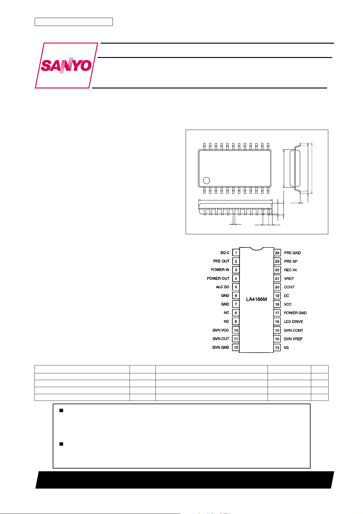
Package Dimensions
unit:mm
3108-MFP24D
15.3
0.4
[LA4166M]
1.27
13
7.9
2.55max
2.250.1
0.67
24
112
Pin Assignment
9.2
10.5
0.25
0.625
SANYO : MFP24D
Specifications
Absolute Maximum Ratings at Ta = 25˚C
retemaraPlobmySsnoitidnoCsgnitaRtinU
egatlovylppuSV
noitapissidrewoPP
egnarerutarepmetgnitarepOrpoT 05+ot01–
egnarerutarepmetegarotSgtsT 051+ot55–
CC
D
21500TH (KT)/D161TS No.3977–1/7
Top view
5.4V
1.1W
˚C
˚C
Page 2
LA4166M
Recommended Operating Conditions at Ta = 25˚C
retemaraPlobmySsnoitidnoCsgnitaRtinU
egatlovylppuSV
egnaregatlovylppuSV
ecnatsiserdaolreifilpmarewoPR
ecnatsiserdaolreifilpmaerPR
CC
CC
1L
2L
Electrical Characteristics at Ta = 25˚C, VCC=3V, power amplifier RL=4Ω (playback mode) or 10kΩ (recording
mode), preamplifier RL=10kΩ, f=1kHz, 0dBm=0.775V unless otherwise noted.
retemaraPlobmySsnoitidnoC
V,edomgnidroceR
tnerrucylppus
niagegatlov
egatlovesiontupnireifilpmaerPV
niagegatlovreifilpmarewoPV
rewoptuptuoreifilpmarewoPP
egatlovtupniNO-nrutCLAV
egnarCLARCLA.1etoneeS038354Bd
noitrotsidcinomrahlatotCLADHT
egatlovtuptuoCLAV
tnerrucevirdDELI
egatlovecnereferronrevoG
tnerructupnitnecseiuqronrevoGI
oitarredividtnerrucronrevoGKI
egatlovtuptuolaudiserronrevoGV
citsiretcarahc
citsiretcarahc
citsiretcarahctnerruc
citsiretcarahc
tnecseiuqreifilpmarewopdnareifilpmaerP
pool-desolcreifilpmarewopdnareifilpmaerP
niagegatlovpool-desolcreifilpmaerPV
egatlovtuptuomumixamreifilpmaerPV
noitrotsidcinomrahlatotreifilpmaerPDHT
noitrotsidcinomrohlatotreifilpmarewoPDHT
egatlovesiontuptuoreifilpmarewoPV
tuptuo.svoitaregatlovecnereferronrevoG
I
OCC
V
1G
2G
O
IN
3G
O
ON
I
O
DEL
V
d
egatlovylppus.svegatlovecnereferronrevoG
egatlovylppus.svoitarredividtnerrucronrevoG
tnerructuptuo.svoitarredividtnerrucronrevoG
1
V
O
2PO
RV0= Ω R,L4= Ω ssapdnabtuptuozHk02otzH02,
V
3
V
I
GERNVG
m
I
m
m
I
tas
m
V
V
I
m
I
m
retlif
R,%01=DHT
R,Wm03=
retlif
NICER
NICER
Am001=1.152.14.1V
Am001= 236Am
V,Am002=
CC
CC
V0=215283Am
I
V,edomkcabyalP
V0=316293Am
I
V,edomgnidroceR
V,edomkcabyalP
V,edomgnidroceR
V,edomkcabyalP
V,edomkcabyalP
R,mBd5–=
4= Ω 0.625.820.13Bd
L
4= Ω 081512053Wm
L
4= Ω 50.05.05.1%
L
mBd04–=1.076.05.1%
mBd04–=53.064.055.0V
DELderagnisU0.15.25.4Am
Am001ot05=540555
mBd5–=0.265.460.76Bd
O
mBd5–=0.175.370.67Bd
O
O
O
O
I,V5.4ot8.1=
m
I,V5.4ot0.2=
m
R,mBd01–=
001= Ω 5.230.535.73Bd
FN
R,mBd01–=
001= Ω 5.240.545.74Bd
%1=DHT,edomkcabyalP3.06.00.1V
V4.0=10.011.00.1%
FERNVG
FN
ssapdnabtuptuozHk02otzH02,edomkcabyalP
V=
TNOCNVG
.2etoneeS,Am001=01.05.0V/%
.3etoneeS,Am001ot05=01.05.0V/%
.4etoneeS,Am002ot05=0700.030.0Am/%
.5etoneeS,Am002ot05=50.0–500.050.0Am/%
nimpytxam
5.01.10.2Vµ
552001Vµ
5.66–0.96–5.17–mBd
1.03.05.0V
3V
6.3ot8.1V
)edomkcabyalP(4
)edomgnidroceR(01kΩ
01kΩ
sgnitaR
Ω
tinU
Notes
1. Referred to ALC turn-ON voltage, input range for the output level to rise 2.5dB
2. The characteristic is given the equation
∆V
GVN REF
V
GVN REF
+ ∆V
CC
3. The characteristic is given by the equation
∆K
+ ∆V
K
CC
4. The characteristic is given by the equation
∆V
GVN REF
V
GVN REF
+ ∆I
m
5. The characteristic is given by the equation
∆K
+ ∆I
K
m
No.3977–2/7
Page 3
Block Diagram
LA4166M
Pin Description
rebmuNemaNnoitpircseD
1CQEnoitcennocroticapacnoitazilauqekcabyalP
2TUOERPtuptuoreifilpmaerP
3NIREWOPtupnireifilpmarewoP
4TUOREWOPtuptuoreifilpmarewoP
5CDCLAnoitcennockrowtenlortnocscitsiretcarahcCLA
7,6DNGdnuorG
9,8CNnoitcennocoN
01VNVG
11TUONVGtuptuoronrevoG
21DNGNVGdnuorgronrevoG
31SVegatlovylppusrotoM
41FERVNVGtuptuoegatlovecnereferronrevoG
51TNOCNVGtupnilortnocronrevoG
61EVIRDDELtuptuorevirdDEL
71DNGREWOPdnuorgreifilpmarewoP
81V
91CDnoitcennocroticapacretlif-elppiR
02TNOCtupnitceleskcabyalpdnadroceR
12FERVtuptuoegatlovecnerefeR
22NICERtupnilangisgnidroceR
32FNERPtupnilortnocniagreifilpmaerP
42DNGERPdnuorgreifilpmaerP
CC
CC
ylppusronrevogV6.3ot8.1
ylppusV6.3ot8.1
Allowable power dissipation, Pd max – W
Pd max – Ta
Ambient temperature, Ta – °C
No.3977–3/7
Page 4

Schematic Diagram
LA4166M
No.3977–4/7
Page 5

Measurement Circuit
LA4166M
Functional Description
The LA4166M comprises a preamplifier, an ALC, an
LED driver, a power amplifier and a governor. The
operation of these fuctional blocks in recording and
playback modes is shown in table 1. Recording mode
is selected when CONT is held at 0V, and playback
mode, when CONT is open.
Table 1. Block operation
edoMreifilpmaerPCLA
gnidroceRNONONONONO
kcabyalPNOFFOFFONONO
DEL
revird
rewoP
reifilpma
ronrevoG
No.3977–5/7
Page 6

T ypical Application
LA4166M
Figure 1. Application circuit
Note the external components are used to determine the
LA4166M operating characteristics. For example, C2
determines the playback equalization characteristic, R8
determines the preamplifier gain, C8 and R4 determine
the ALC attack and recovery times and C17 determines
the power supply ripple rejection. The ripple rejection
decreases as the capacitance C17 is decreased.
Other components are used to determine the overall circuit characteristics. For example, C1 and R1 determine
the recording current and C7 prevents output oscillations.
Note also that LA4166M internal components determine
other LA4166M characteristics. For example, the 2.2kΩ
PRE IN input resistor determines the ALC range, and
the 1kΩ and 30kΩ resistors at the power amplifier inverting input determine amplifier gain.
In addition, LED DRIVE should be left open when not
using the LED indicator function, the double-pole switch
that controls LED DRIVE is normally closed, the NC
pins should be left open, and the GND pins should be
tied to ground
No.3977–6/7
Page 7

LA4166M
Specifications of any and all SANYO products described or contained herein stipulate the performance,
characteristics, and functions of the described products in the independent state, and are not guarantees
of the performance, characteristics, and functions of the described products as mounted in the customer's
products or equipment. To verify symptoms and states that cannot be evaluated in an independent device,
the customer should always evaluate and test devices mounted in the customer's products or equipment.
SANYO Electric Co., Ltd. strives to supply high-quality high-reliability products. However, any and all
semiconductor products fail with some probability. It is possible that these probabilistic failures could
give rise to accidents or events that could endanger human lives, that could give rise to smoke or fire,
or that could cause damage to other property. When designing equipment, adopt safety measures so
that these kinds of accidents or events cannot occur. Such measures include but are not limited to protective
circuits and error prevention circuits for safe design, redundant design, and structural design.
In the event that any or all SANYO products(including technical data,services) described or
contained herein are controlled under any of applicable local export control laws and regulations,
such products must not be exported without obtaining the export license from the authorities
concerned in accordance with the above law.
No part of this publication may be reproduced or transmitted in any form or by any means, electronic or
mechanical, including photocopying and recording, or any information storage or retrieval system,
or otherwise, without the prior written permission of SANYO Electric Co. , Ltd.
Any and all information described or contained herein are subject to change without notice due to
product/technology improvement, etc. When designing equipment, refer to the "Delivery Specification"
for the SANYO product that you intend to use.
Information (including circuit diagrams and circuit parameters) herein is for example only ; it is not
guaranteed for volume production. SANYO believes information herein is accurate and reliable, but
no guarantees are made or implied regarding its use or any infringements of intellectual property rights
or other rights of third parties.
This catalog provides information as of February, 2000. Specifications and information herein are subject
to change without notice.
PS No.3977–7/7
 Loading...