

Page 1

Any and all SANYO products described or contained herein do not have specifications that can handle
applications that require extremely high levels of reliability, such as life-support systems, aircraft’s
control systems, or other applications whose failure can be reasonably expected to result in serious
physical and/or material damage. Consult with your SANYO representative nearest you before using
any SANYO products described or contained herein in such applications.
SANYO assumes no responsibility for equipment failures that result from using products at values that
exceed, even momentarily, rated values (such as maximum ratings, operating condition ranges,or other
parameters) listed in products specifications of any and all SANYO products described or contained
herein.
Monolithic Linear IC
Single-Chip Tape Recorder Audio System
Ordering number:ENN870D
LA4160
SANYO Electric Co.,Ltd. Semiconductor Company
TOKYO OFFICE Tokyo Bldg., 1-10, 1 Chome, Ueno, Taito-ku, TOKYO, 110-8534 JAPAN
Features
• A single package contaning preamplifier, ALC circuit,
power amplifier.
• Preamplifier with high gain, and power amplifier with
high gain and output.
1W typ. (VCC=6V, RL=4Ω)
2.2W typ. (VCC=9V, RL=4Ω)
• Minimum number of external parts required.
• Soft tone quality at the time of output saturation.
• Wide range of ALC and small variation in output voltage.
• Wide range of operating supply voltage.
• Small shock noise at the time of supply voltage ON/OFF
(With built-in prevention circuit).
• Variable monitor capability due to recording amplifier
consisting of preamplifier alone.
Specifications
Absolute Maximum Ratings at Ta = 25˚C
retemaraPlobmySsnoitidnoCsgnitaRtinU
egatloVylppuSmumixaMV
noitapissiDrewoPelbawollAxamdP
erutarepmeTgnitarepOrpoT 57+ot02–
erutarepmeTegarotSgtsT 051+ot04–
xam 31V
CC
05 × 05 × mm5.1
Package Dimensions
unit:mm
3005A-DIP14T
[LA4160]
2.5
2.1
14
1
6.0
1.53
1.88 2.54
3
detaoc-uC52.2W
19.06.5
0.5
8
7.62
7
3.46
0.51min
1.3
SANYO : DIP14T
6.45
0.4
4.26max
3.5
2.1W
˚C
˚C
Recommended Operating Conditions at Ta = 25˚C
retemaraPlobmySsnoitidnoCsgnitaRtinU
egatloVylppuSV
ecnatsiseRdaoLR
CC
L
12800TH (KT)/41594HK/O207TA/4015KI/8171KI, TS No.870–1/11
9ot6V
Ω
8ot2.3
Page 2

LA4160
Operating Characteristics at Ta = 25˚C, VCC=6V, f=1kHz, See specified Test Circuit
retemaraPlobmySsnoitidnoC
tnerruCtnecseiuQI
]reifilpmaerP[
niaGegatloVGV
egatloVtuptuOmumixaMV
ecnatsiseRtupnIr
egatloVesioNtupnItnelaviuqEV
leveLtupnICLACLAkcabyalP,%1=DHT02–21–mBd
]reifilpmarewoP[
niaGegatloVGVR,pooLdesolC
rewoPtuptuOP
noitrotsiDcinomraHlatoTDHTPoWm052=3.05.1%
ecantsiseRtupnIr
egatloVesioNtuptuOV
noitcejeRelppiRR
Test Circuit Diagram
VCCV6=8103Am
OCC
VCCV9=3204Am
poolnepO58Bd
kcabyalP,pooldesolC04Bd
O
i
IN
O
i
ON
r
kcabyalP0.10.2Vµ
V
CC
V
CC
V
CC
k01=gR Ω 6.08.1Vm
V,0=gR
R
kcabyalP,%1=DHT9.02.1V
15= Ω 345474Bd
f
%01=DHT,V6=7.00.1W
%01=DHT,V5.7=0.15.1W
%01=DHT,V9=7.12.2W
zH001=f,Vm051=0454Bd
sgnitaR
nimpytxam
1203kΩ
03kΩ
tinU
Test Method
metI
I
GV2ffoffoffononoffoffoD,A
P
o
DHT2ffoffoffononoffoffoD VegatlovtuptuotaDHTtseT
V
Power amplifier
ON
V
RN
V
OG
Voxam1ffoffoffononoffoffoB .%1=DHTtaegatlovtuptuotseT
V
IN
preamplifier
hctiwS
1WS2WS3WS4WS5WS6WS7WS8WS
OCC
level
–nonoffononoffoffo– .tnerructiucrictseT
2ffoffoffononoffoffoD
–noffoffononoffoffoD .egatlovesiontuptuotseT
–noffoffononoffoffoD
1ffoffonoffonoffoffoB,AVgol02
–ffonoffonononoffoC
tupnICLA
1ffoffoffoffoffoffonoB,A.%1=DHTtaegatlovtupnitseT
tseT
aera
Vgol02
oV/i
Vegatlovtuptuo
o
.)Bd(
oV/i
dohtemtseT
Vsiegatlovtupnierehw,)Bd(
,
.
.tuptuootnititevnoc
o
.zHk1taniaggnisu
i
dna%01=DHTtaegatlovtuptuotseT
.V1=
noVm051)zH001(elppiresoprepuS
.elppirtuptuotsetdnaegattovylppus
ybk2.2=gRtaegatlovesiontuptuotrevnoC
No.870–2/11
Page 3

Equivalent Circuit Block Diagram
LA4160
Sample Application Circuit 1 : Cassette Recorder
No.870–3/11
Page 4
LA4160
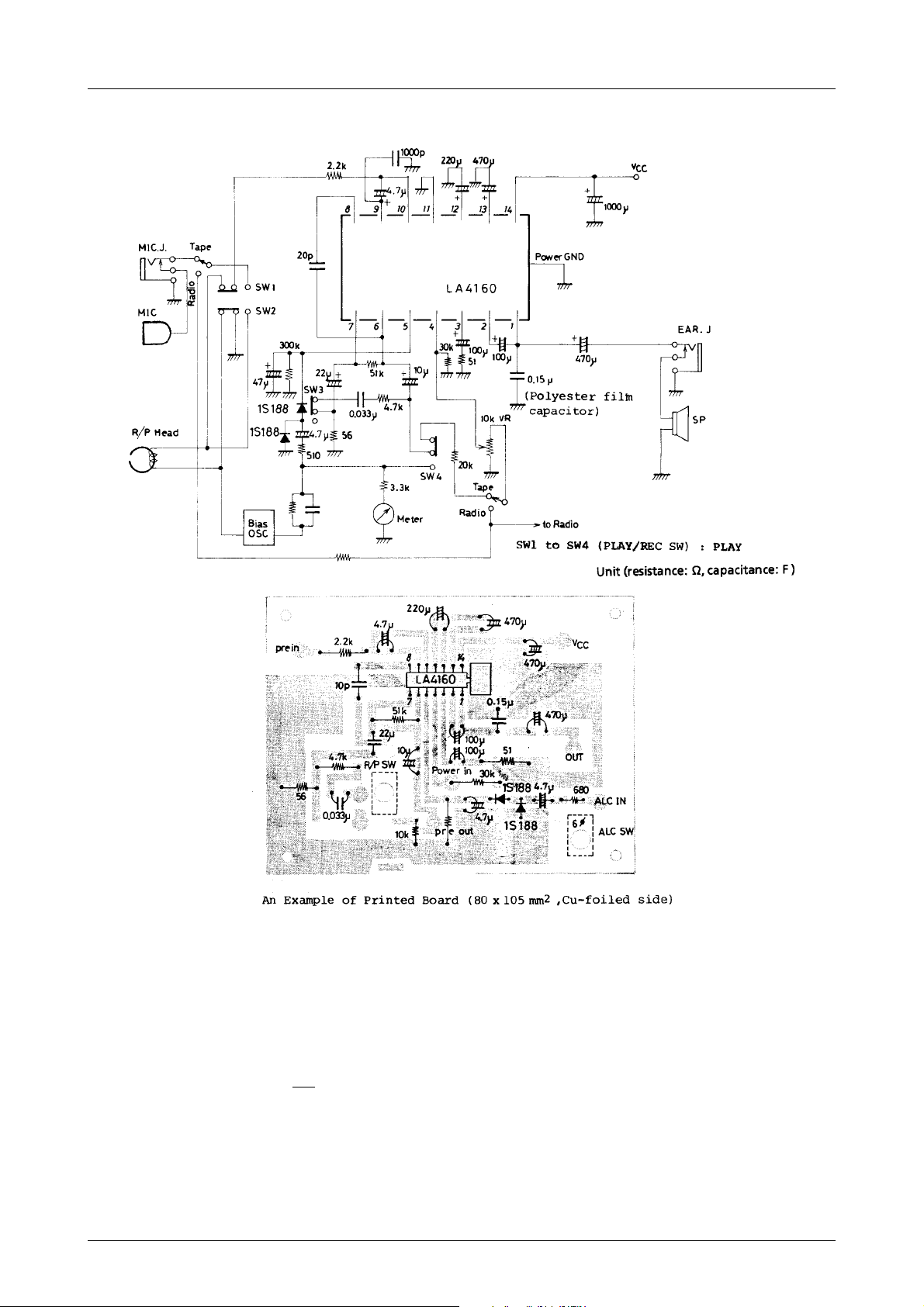
Sample Application Circuit 2 : Radio-Cassette Recorder
Description of Application Circuit
1. Preamplifier
The preamplifier circuit consists of the input differential stage (TR9, 10), level shift stage (TR13), and output
stage (TR17, 18, 19). Since the output stage is of push-pull type, no remarkable drop in the output voltage
occurs even at low load impedances and the output can be connected direct to the ALC circuit and meter circuit.
The external DC/AC feedback resistor (Z2) can be set arbitrarily and the closed loop gain is obtained by the
following equation.
VG (pre) 20 log ( ) (dB)
The input impedance depends on internal resistance R2 which is 30kΩ.
Z2
Z1
No.870–4/11
Page 5

Preamplifier Circuit
LA4160
Since the maximum output voltage for THD=1% drops at less than 600Ω of the composite load impedance
viewed from output pin (6), it is desirable to make the composite load impedance more than 600Ω when using
this IC. (Refer to VO max, THD – RL characteristics.)
2. ACL Circuit
The ALC circuit is of Darlington configuration which consists of TR1, 2. The collector-to-emitter impedance of
TR1 made variable by the DC voltage to be applied to control pin (5) and the input voltage of the preamplifier
is controlled. Whe the DC voltage to be applied to pin (5) is set at approximately 1.1V, TR1, 2 are turned ON
and ALC is turned ON. For the rectifier circuit, it is recommended to use the voltage doubler rectifirer which is
excellent in compression ratio. For the sets of 6V VCC, it is recommended to use a germanium diode so that the
ALC width can be made wider even at the time of decreased voltages.
No.870–5/11
Page 6

LA4160
3. Power Amplifier
The power amplifier circuit consists of the differential stage (TR22, 23), predriver stage (TR41), driver stage
(TR42, 44), and output stage (TR47,48). Bias resistor R36 of TR20 at the first stage is attached externally and
the input impedance depends on this R36. Input pin (4) whose potential is nearly equal to the ground potential
can be connected direct to the variable resistor without using an input coupling capacitor. The closed loop
voltage gain is obtained by the following equation.
VG (pwr)=20log
Since R19=20kΩ, R18=50Ω are set, approximately 52dB max. is available if Rf=0 is taken.
Proper Cares in Using IC
1. Printed Circuit Board
For the printed circuit board layout, refer to the printed circuit pattern example in principle. It is necessary that
the grounding points of the power amplifier input (variable resistor), pin (3) feedback resistor (Rf), and bias
resistor (R35) should be adjacent to one another. Especially, it should be noted that if a common impedance
exists in the variable resistor grounding, the distortion, residual ripple, and cross interference (leak of signal
between preamplifier and power amplifier) may worsen.
R19
(R18+Rf)
No.870–6/11
Page 7

LA4160
2. Oscillation
a) Preamplifier
Since oscillation may osccur when used at a low
voltage gain, a capacitor of approximately 10pF
must be connected across pins (8) and (6) for
phase compensation. If the capacitor connected
across pins (8) and (6) has a large capacitance at
a low load impedance, further oscillation may
occur, and in this case the load pin must be
grounded through a capacitor of approximately
0.01µF (Polyester film capacitor). The input pin
must be grounded through a capacitor of approximately 1000pF for the purpose of prevention of radio
disturbance and oscillation.
b) Power Amplifier
For the oscillation preventing capacitor connected across output pin (1) and ground, it is recommended to
use a polyester film capacitor which is excellent in temperature characteristic and frequency characteristic. It
should be noted, however, that if such a polyester film capacitor as to have a resonance point at a high
frequency is used oscillation may not be prevented.
3. Shock Noise
The shock noise which occurs from the power amplifier at the time of power supply ON/OFF is reduced by
means of the prevention circuit. However, when the starting time of the power amplifier is set earlier than that
of the preamplifier or the power supply is turned ON immediately after turning OFF, it may happen that the
shock noise of the preamplifier cannot be masked. In this case, a germanium diode is connected across pins (7)
and (9), and pins (7) and (12) respectively to make the starting time as early as possible. Even if no germanium
diode is connected across pins (7) and (12), the starting time can be made earlier, but the starting time can be
made much earlier by using 2pcs. of germanium diode.
4. Power Supply for Radio’s Built-in Capacitor Microphone
Pin (13) is for the low ripple power supply. This pin cannot be used as the power supply for a block, such as
radio, which requires a large amount of current. The reason for this is that if this pin is used for this purpose,
the middle point of the power amplifier shifts, thereby causing the drop in output. However, this pin can be
safely used as the power supply for a built-in capacitor microphne.
5. Recording Muting
The recording muting at the time of recording by use of the built-in microphone is enabled by applying 1 to 5V
DC voltage to feedback pin (3) of the power amplifier. (Power amplifier : Cutoff)
No.870–7/11
Page 8

LA4160
6. In case of using in a radio-cassette recorder, the IC and the bar antenna must be arranged sufficiently distant
from each other to avoid the radiation of higher harmonic component at the time of output saturation of the
power amplifier.
7. Pin-to-pin short causes breakdown and deterioration.
8. Load short causes breakdown and deterioration of both preamplifier and power amplifier.
No.870–8/11
Page 9

LA4160
No.870–9/11
Page 10

LA4160
No.870–10/11
Page 11

LA4160
Specifications of any and all SANYO products described or contained herein stipulate the performance,
characteristics, and functions of the described products in the independent state, and are not guarantees
of the performance, characteristics, and functions of the described products as mounted in the customer's
products or equipment. To verify symptoms and states that cannot be evaluated in an independent device,
the customer should always evaluate and test devices mounted in the customer's products or equipment.
SANYO Electric Co., Ltd. strives to supply high-quality high-reliability products. However, any and all
semiconductor products fail with some probability. It is possible that these probabilistic failures could
give rise to accidents or events that could endanger human lives, that could give rise to smoke or fire,
or that could cause damage to other property. When designing equipment, adopt safety measures so
that these kinds of accidents or events cannot occur. Such measures include but are not limited to protective
circuits and error prevention circuits for safe design, redundant design, and structural design.
In the event that any or all SANYO products(including technical data,services) described or
contained herein are controlled under any of applicable local export control laws and regulations,
such products must not be exported without obtaining the export license from the authorities
concerned in accordance with the above law.
No part of this publication may be reproduced or transmitted in any form or by any means, electronic or
mechanical, including photocopying and recording, or any information storage or retrieval system,
or otherwise, without the prior written permission of SANYO Electric Co. , Ltd.
Any and all information described or contained herein are subject to change without notice due to
product/technology improvement, etc. When designing equipment, refer to the "Delivery Specification"
for the SANYO product that you intend to use.
Information (including circuit diagrams and circuit parameters) herein is for example only ; it is not
guaranteed for volume production. SANYO believes information herein is accurate and reliable, but
no guarantees are made or implied regarding its use or any infringements of intellectual property rights
or other rights of third parties.
This catalog provides information as of January, 2000. Specifications and information herein are subject
to change without notice.
PS No.870–11/11
 Loading...