

SANYO LA4145 Datasheet
Ordering number: EN1339D
Monolithic Linear IC
LA4145
0.6 to 0.9 W AF Power Amplifier
for Radio Cassette Recorders
Features
.
The LA4145 is especially suited for use in cassette tape
recorder, radio-cassette, recorder, stereo cassette player
applications.
.
0.6 W typ/VCC= 6.0 V, RL=8Ω, THD = 10%
0.9 W typ/V
.
Minimum number of external parts required
.
Soft clip
.
Small pop noise at VCCON/OFF mode
.
Voltage gain fixed at 50 dB.
An external resistor can be connected to reduce this value.
= 6.0 V, RL=4Ω, THD = 10%
CC
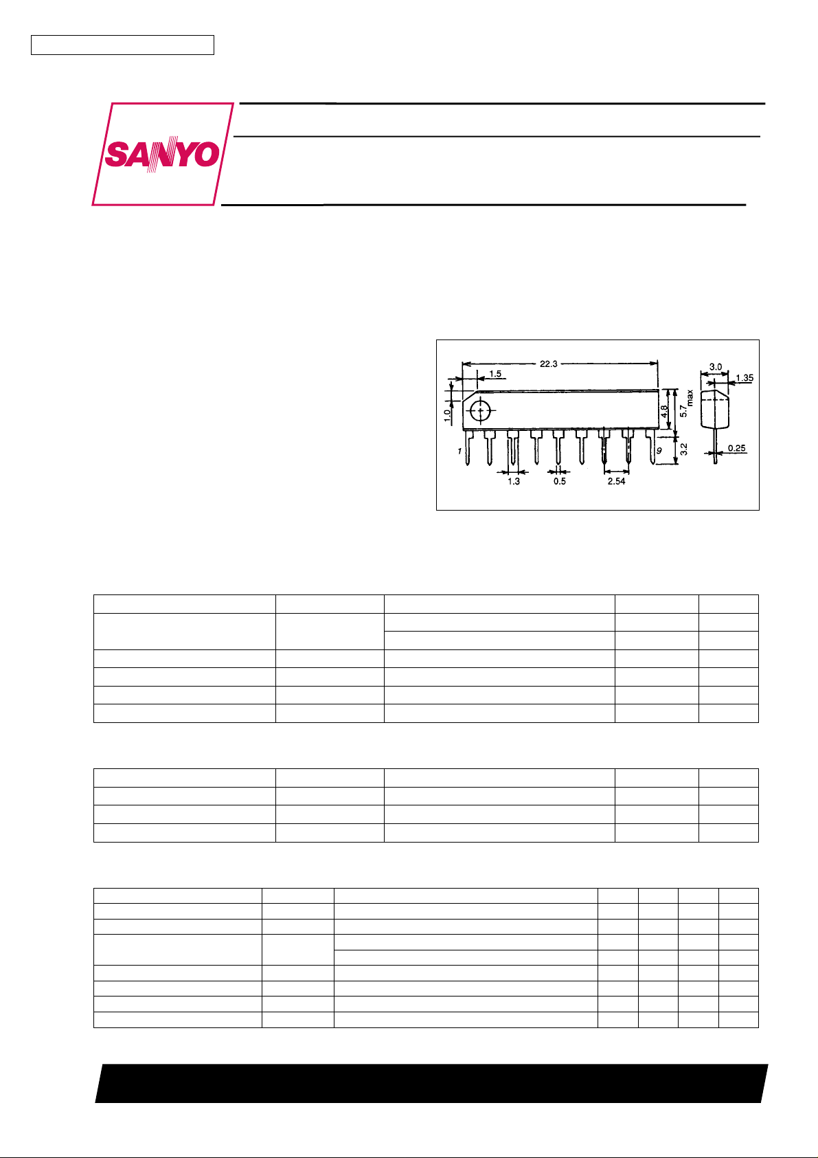
Package Dimensions
unit : mm
3017C-SIP9
[LA4145]
SANYO : SIP9
Specifications
Maximum Ratings at Ta = 25°C
Parameter Symbol Conditions Ratings Unit
Maximum supply voltage V
Maximum output current I
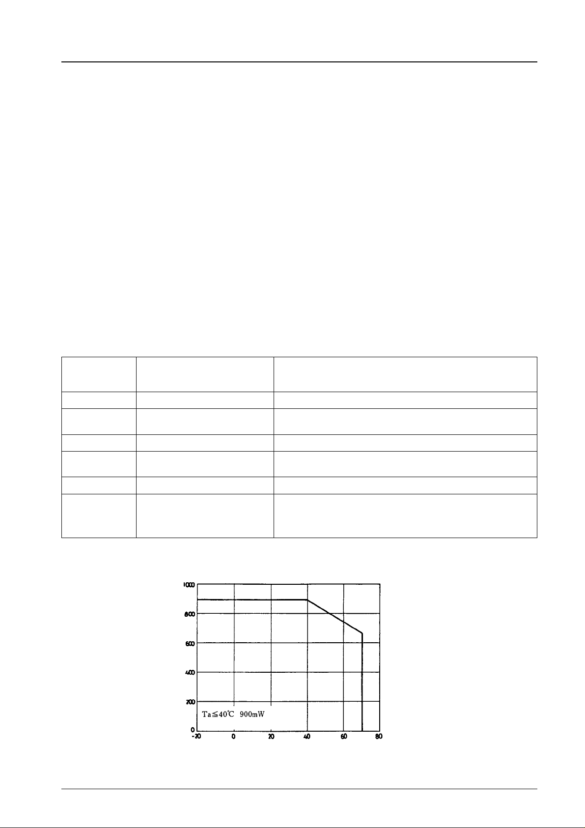
Allowable power dissipation Pd max 50 × 50 mm
Operating temperature Topr –20 to +70 °C
Storage temperature Tstg –40 to +150 °C
max
CC
peak 500 mA
O
Quiescent mode 9 V
Operating mode R
=8Ω 8V
L
2
with PCB 0.9 W
Operating Conditions at Ta = 25°C
Parameter Symbol Conditions Ratings Unit
Recommended supply voltage V
Recommended load resistance R
Operating voltage range V
CC
L
CC
6V
4to8 Ω
3.6 to 8 V
Operating Characteristics at Ta = 25°C, VCC= 6.0 V, RL=8Ω,Rg=600Ω,f=1kHz
Parameter Symbol Conditions min typ max Unit
Quiescent current I
Voltage gain VG 48 50 52 dB
Output power P
Total harmonic distortion THD P
Input resistance r
Output noise voltage V
Ripple rejection ratio SVRR Rg = 0, f
CCO
NO
LA4145 10 20 mA
THD = 10%, RL=4Ω 0.9 W
O
THD = 10%, R
= 0.1 W 0.2 1.0 %
O
i
Rg=10kΩ, B.P.F. = 20 Hz to 20 kHz 0.6 1.2 mV
=8Ω 0.45 0.6 W
L
30 kΩ
= 100 Hz, VR= 150 mV –35 –40 dB
R
SANYO Electric Co.,Ltd. Semiconductor Bussiness Headquarters
TOKYO OFFICE Tokyo Bldg., 1-10, 1 Chome, Ueno, Taito-ku, TOKYO, 110 JAPAN
53096HA(II)/O217KI/N055MW/4034/N163KI,TS No.1339-1/5
LA4145
Proper care in changing voltage gain
An external resistor can be connected in series with the feedback capacitor at pin 2 to reduce the voltage gain.
(See RNF-VG characteristic.)
IC usage notes
1. Maximum ratings
If the IC is used in the vicinity of the maximum ratings, even a slight variation in conditions may cause the maximum ratings
to be exceeded, thereby leading to breakdown. Allow an ample margin of variation for supply voltage, etc. and use the IC in
the range where the maximum ratings are not exceeded.
2. Pin-to-pin short
If power is applied when the space between pins is shorted, breakdown or deterioration may occur. When mounting the IC on
the board or applying power, make sure that the space between pins is not shorted with solder, etc.
3. Radio applications
For use in radio applications, keep a good distance between IC and bar antenna.
4. Printed circuit pattern
When designing the printed circuit pattern, make the power supply, output, and ground lines thicker and shorter and
determine the pattern and parts placement so that no feedback loop is formed between input and output. Place power
capacitor C
(See the sample printed circuit pattern.)
, oscillation blocking capacitor C3as close to the IC pin as possible to prevent oscillation from occurring.
6
Description of external parts
C1(47 µF) Feedback capacitor (NF capacitor) Low cutoff frequency fLdepends on this capacitor.
C
(100 µF) Bootstrap capacitor
2
C
(0.15 µF) Oscillation blocking capacitor It is recommended to use a polyester film capacitor being good in
3
C
(470 µF) Output capacitor
4
C
(47 µF) Decoupling capacitor Serves to reject ripple. The starting time depends on this capacitor.
5
C
(470 µF) Power capacitor Place as close to the power pin of the IC as possible.
6
R
(30 kΩ) Input bias resistor Serves to apply input bias. The input impedance almost entirely
1
f
=90HzforC1=47µF.
L
Decreasing the capacitor value makes the starting time earlier.
temperature characteristic, high frequency characteristic.
Increasing the capacitor value makes the starting time later.
depends on this resistor value. If a variable resistor also serves for this
purpose, this resistor can be omitted. In this case, it is recommended
to use a resistor of 30 kΩ.
Pd max − Ta
50 × 50 mm2PCB
Allowable power dissipation, Pd max − mW
Ambient temperature, Ta – °C
No.1339-2/5
 Loading...