

SANYO LA2232M, LA2232 Datasheet

Overview
The LA2232 and LA2232M are RDS demodulator ICs
that provide both a 57 kHz bandpass filter as well as ARISK and DK signal recognition functions on chip. Costeffective RDS decoder systems can be constructed by
using an LA2232 or 2232M in conjunction with a
synchronization and error detection/correction LSI from
the LC7070 series. The LA2232 and 2232M provide
improved sensitivity LA2230 and 2230M.
Applications
• RDS signal demodulation
• ARI signal demodulation and SK and DK recognition
Functions
• 57 kHz bandpass filter
• RDS signal demodulation
• Bit rate clock regeneration
• RDS identification output
• ARI signal demodulation
• SK identification output
• DK identification output
• Adjustable ARI detection sensitivity
Features
• High RDS demodulation sensitivity
• Reduced costs and PCB area due to the inclusion of an
on-chip 57 kHz bandpass filter
• Supports improved interference rejection characteristics
by providing ARI detection sensitivity adjustment
• Quick operation startup due to a built-in rapid charging
circuit for use at power application.
Package Dimensions
unit: mm
3067-DIP24S
unit: mm
3112-MFP24S
Ordering number : EN4416A
21097HA(OT) No. 4416-1/9
SANYO: DIP24S
[LA2232]
SANYO: MFP24S
[LA2232M]
SANYO Electric Co.,Ltd. Semiconductor Bussiness Headquarters
TOKYO OFFICE Tokyo Bldg., 1-10, 1 Chome, Ueno, Taito-ku, TOKYO, 110 JAPAN
RDS Decorder
LA2232, 2232M
Monolithic Linear IC

No. 4416A-2/9
LA2232, 2232M
Specifications
Maximum Ratings at Ta = 25°C
Parameter Symbol Conditions Ratings Unit
Maximum supply voltage V
CC
max Pins 13, 14, 15, 23 12 V
LA2232: Ta ≤ 80°C 450 mW
Allowable power dissipation Pd max LA2232M: Ta ≤ 37.5°C 450 mW
LA2232M: Ta = 80°C 280 mW
Entering current I
LED
Pins 13, 14, 15 20 mA
Operating temperature Topr –30 to +80 °C
Storage temperature Tstg
LA2232 –40 to +125 °C
LA2232M –40 to +150 °C
Operating Conditions at Ta = 25°C
Parameter Symbol Conditions Ratings Unit
Recommended supply voltage V
CC
Pin 23 5.0 V
Operating voltage range V
CC
op Pin 23 4.7 to 5.5 V
Operating Characteristics at Ta = 25°C, VCC= 5.0 V
Ratings
Parameter Symbol
min typ max
Unit
Quiescent current 14 22 28 mA
Band pass filter gain f = 57 kHz 9 12.5 17 dB
f = 60 kHz (57 kHz = 0 dB) –6 –2.5 0 dB
Band pass filter selectivity f = 54 kHz (57 kHz = 0 dB) –6 –3.5 0 dB
f = 38 kHz (57 kHz = 0 dB) –39 –33 dB
PLL capture range 5 mVrms CW input
–0.5 %
+0.8 %
RDS detection sensitivity The pin 6 input when pin 15 goes low 0.4 1.0 mVrms
SK detection sensitivity The pin 6 input when pin 14 goes low 1.0 2.0 mVrms
DK detection sensitivity The pin 6 input when pin 13 goes low 1.1 2.0 mVrms
The maximum input on pin 6 for the (ARI + RDS)
30 50 mVrms
RDS
signal when pin 15 goes low
Input dynamic range
The maximum input on pin 6 for the RDS signal
250 mVrms
when pin 15 goes low
DK
The maximum input on pin 6 for the ARI signal
75 100 mVrms
when pin 15 goes low
Bit rate clock jitter ±8 ±9 ±10 µs
RDS lockup time
The time until pin 15 goes low following RDS
35 ms
becoming a 3 mV input
SK lockup time
The time until pin 14 goes low following ARI 45 ms
becoming an 8 mV input
SK + RDS lockup time
The time until pin 15 goes low following RDS +
80 ms
ARI becoming an 8.5 mV input
Data output
The high level for pin 17 4.7 4.9 5.0 V
The low level for pin 17 0 0.1 0.3 V
Bit rate clock output
The high level for pin 18 4.7 4.9 5.0 V
The low level for pin 18 0 0.1 0.3 V
VCO free-running frequency 453 456 459 kHz
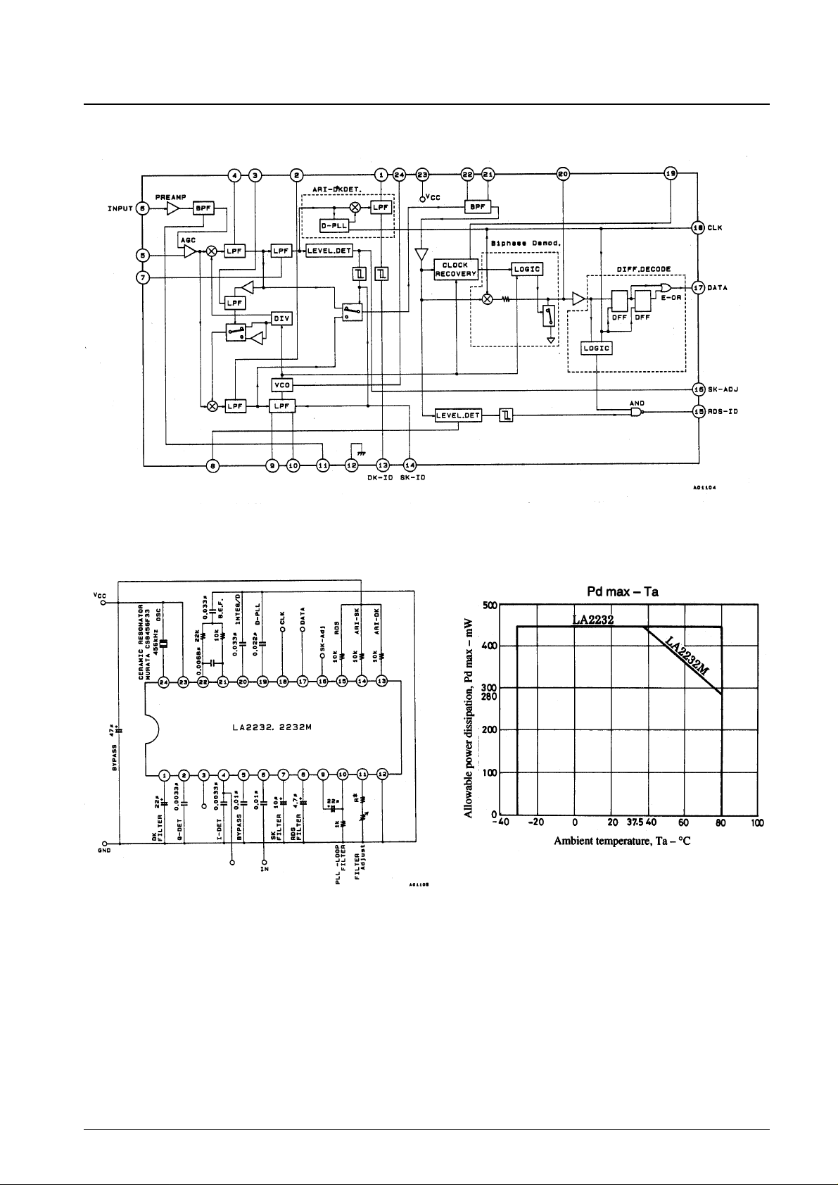
Equivalent Circuit Block Diagram
Test Circuit
No. 4416A-3/9
LA2232, 2232M
*R = 6.8 kΩ (for the LA2232)
R = 5.6 kΩ (for the LA2232M
Unit (resistance: Ω, capacitance: F)
 Loading...