

Page 1
Any and all SANYO products described or contained herein do not have specifications that can handle
applications that require extremely high levels of reliability, such as life-support systems, aircraft’s
control systems, or other applications whose failure can be reasonably expected to result in serious
physical and/or material damage. Consult with your SANYO representative nearest you before using
any SANYO products described or contained herein in such applications.
SANYO assumes no responsibility for equipment failures that result from using products at values that
exceed, even momentarily, rated values (such as maximum ratings, operating condition ranges,or other
parameters) listed in products specifications of any and all SANYO products described or contained
herein.
MOSFET : P-Channel Silicon MOSFET
SBD : Schottky Barrier Diode
DC/DC Converter Applications
Ordering number:ENN5372A
FX856
SANYO Electric Co.,Ltd. Semiconductor Company
TOKYO OFFICE Tokyo Bldg., 1-10, 1 Chome, Ueno, Taito-ku, TOKYO, 110-8534 JAPAN
Features
· The FX856 composite device consists of following
two devices to facilitate high-density mounting. One
is a P-channel MOSFET that features low ON
resistance, high-speed switching, and low driving
voltage. The other is a shottky barrier diode that
features short reverse recovery time and low forward
voltage.
· Each device incorporated in the FX856 is equivalent
to the 2SJ416 and to the SB07-03P, respectively.
Specifications
Absolute Maximum Ratings at Ta = 25˚C
retemaraPlobmySsnoitidnoCsgnitaRtinU
]TEFSOM[
egatloVecruoS-ot-niarDV
egatloVecruoS-ot-etaGV
)CD(tnerruCniarDI
)esluP(tnerruCniarDI
noitapissiDrewoPelbawollAP
erutarepmeTlennahChcT 051
erutarepmeTegarotSgtsT 051+ot55–
]DBS[
egatloVesreveRkaePevititepeRV
egatloVegruSesreveRkaePevititeper-noNV
tnerruCdeifitceRegarevAI
tnerruCdrawroFegruSI
erutarepmeTnoitcnuJjT 521+ot55–
erutarepmeTegarotSgtsT 521+ot55–
Marking : 863
SSD
SSG
D
PD
Mounted on a ceramic board (750mm2×0.8mm)
D
Tc=25°C
MRR
MSR
O
MSF
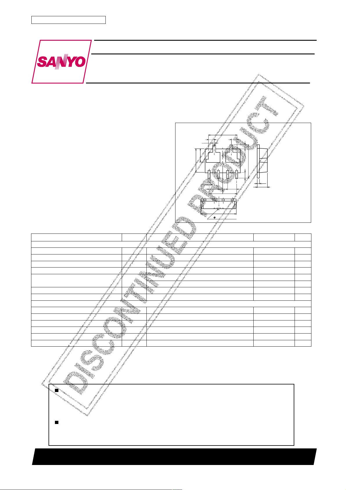
Package Dimensions
unit:mm
2119
[FX856]
5.0
1.5
0.5
2.4
4.2
4
0.4
0.8
%1elcycytud,sµ01WP 8–A
elcyc1,evaweniszH05 5A
1.5
56
32
0.8
2.4
2.4
6.2
1.2D 0.15max
0.7
5.9
1.0
1
0.4
1.8
1 : Gate
2 : Source
3 : No Contact
4 : Anode
5 : Cathode
6 : Drain
(Bottom view)
SANYO : XP6
03–V
02±V
2–A
5.1W
6W
˚C
˚C
03V
53V
007Am
˚C
˚C
92500TS (KOTO) TA-2770 No.5372–1/5
Page 2
FX856
Electrical Characteristics at Ta = 25˚C
retemaraPlobmySsnoitidnoC
]TEFSOM[
egatloVnwodkaerBecruoS-ot-niarDV
tnerruCniarDegatloVetaG-oreZI
tnerruCegakaeLecruoS-ot-etaGI
egatloVffotuCV
ecnattimdArefsnarTdrawroF|sfy|VSDI,V01–=
R
ecnatsiseRetatS-nOecruoS-ot-niarDcitatS
R
ecnaticapaCtupnIssiCV
ecnaticapaCtuptuOssoCV
ecnaticapaCrefsnarTesreveRssrCV
emiTyaleDNO-nruTt
emiTesiRt
emiTyaleDFFO-nruTt
emiTllaFt
egatloVdrawroFedoiDV
]DBS[
egatloVesreveRV
egatloVdrawroFV
tnerruCesreveRI
ecnaticapaClanimretretnICV
emiTyrevoceResreveRt
ecnatsiseRlamrehTa-jhtR 001
d
d
I
SSD)RB(
D
V
SSD
V
SSG
)ffo(VSDI,V01–=
SG
1)no(IDV,A1–=
SD
2)no(IDV,A1–=
SD
)no(tiucriCtseTdeificepseeS01sn
r
)ffo(tiucriCtseTdeificepseeS011sn
f
I
DS
S
I
R
R
I
F
F
VRV51= 08Aµ
R
IFI=
rr
Mounted on a ceramic board (750mm
V,Am1–=
0=03– V
SG
V,V03–=
SD
SG
SD
SD
SD
V,A2–=
Aµ003=03V
Am007= 55.0V
R
R
0=001– Aµ
SG
V,V61±=
0=01±Aµ
SD
Am1–=0.1– 5.2– V
D
A1–=2.10.2S
D
V01–=013044mΩ
SG
V4–=084056mΩ
SG
zHM1=f,V01–=071Fp
zHM1=f,V01–=021Fp
zHM1=f,V01–=03Fp
tiucriCtseTdeificepseeS02sn
tiucriCtseTdeificepseeS57sn
0=0.1– 2.1– V
SG
elcyczHM1=f,V01=62Fp
sgnitaR
nimpytxam
tiucriCtseTdeificepseeS,Am001= 01sn
2
×0.8mm)
tinU
˚C/W
Electrical Connection
65
1 : Gate
2 : Source
3 : No Contact
4 : Anode
123
4
5 : Cathode
6 : Drain
Switching Time Test Circuit Trr Test Circuit
[MOSFET] [SBD]
VDD= --15V
Duty≤10%
10µs
50Ω 100Ω 10Ω
0V
--10V
PW=10µs
D.C.≤1%
P.G
V
IN
V
IN
G
50Ω
D
ID= --1A
RL=15Ω
V
FX856
S
OUT
VR
--5V
100mA100mA
10mA
t
rr
No.5372–2/5
Page 3
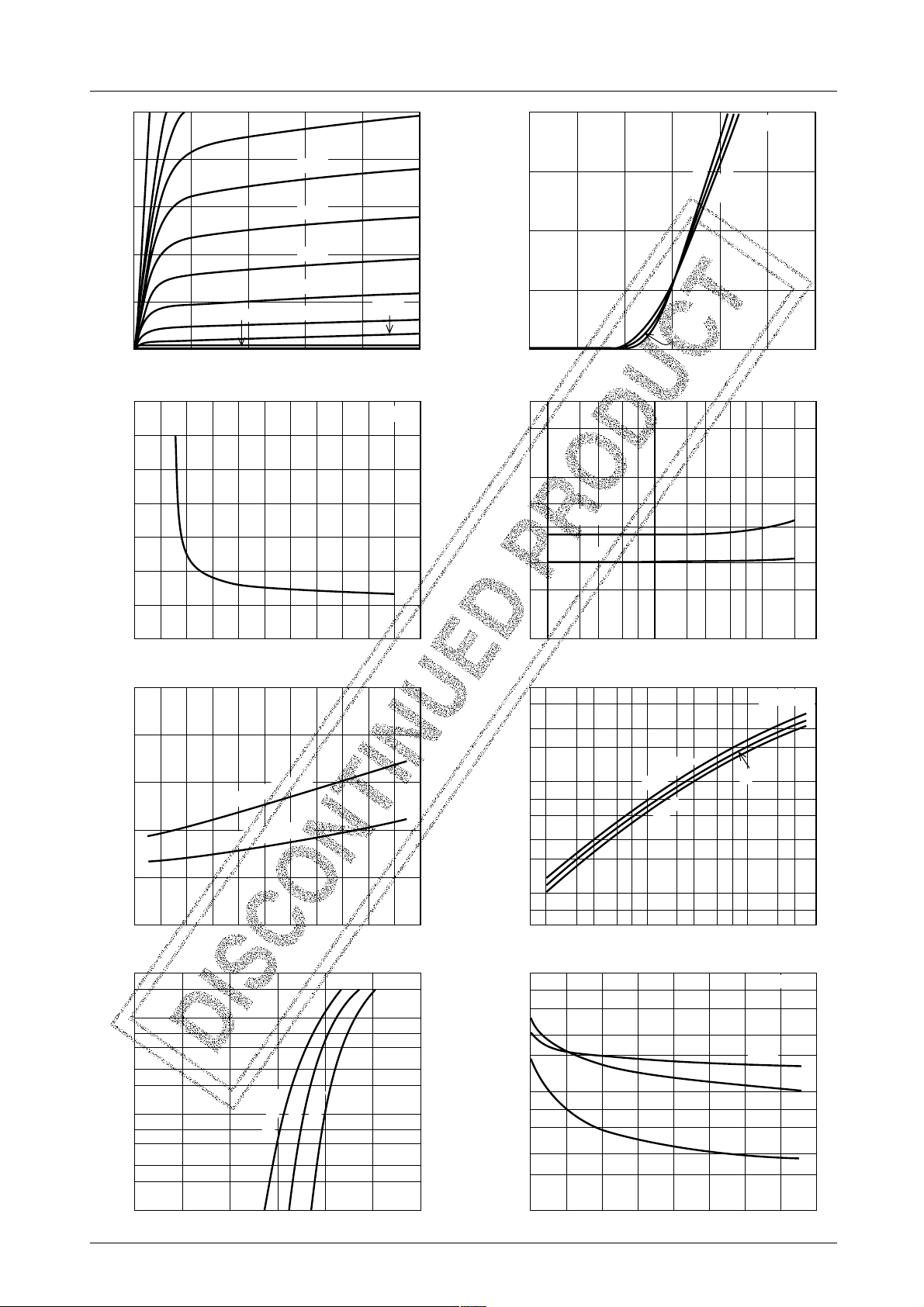
FX856
I
I
-- V
D
--2 .0
--1 .6
--10V
--4.0V
--3.6V
DS
--3.4V
--3.2V
– A
D
--1 .2
--0 .8
--3.0V
--2.8V
[MOSFET] [MOSFET]
--4
--3
– A
D
--2
D
-- V
GS
VDS= --10V
--25°C
Ta=75°C
Drain Current, I
--0 .4
VGS= --2.0V
0
0
--2 --4 --6 -- 8 --1 0
--2.6V
--2.4V
Drain-to-Source Voltage, VDS– V
1.4
1.2
– Ω
1.0
(on)
DS
0.8
0.6
0.4
0.2
Static Drain-to-Source
On-State Resistance, R
0
0 --2 --4 --6 --8 --10 --12 --14 --16 --18 --20 --22
RDS(on) -- V
Gate-to-Source Voltage, V
1.0
0.8
RDS(on) -- Ta
GS
GS
– Ω
(on)
0.6
DS
0.4
0.2
Static Drain-to-Source
On-State Resistance, R
--600--40 --20 0 20 40 60 80 100 120 160140
3
2
--1 .0
7
– A
5
F
3
2
--0 .1
7
5
Forward Current, I
3
2
--0.01
= --1A, V
I
D
= --1A, V
I
D
Ambient Temperature, Ta –˚C
I
F
Diode Forward Voltage, VSD– V
GS
-- V
Ta=75
--0.6 --0.8 --1.2--1 .00 --0.2 --0.4
GS
°C
=4V
=10V
SD
25°C
°C
--25
Drain Current, I
--1
--2.2V
0
0 --1 --2 --3 --4 --5 --6
IT01328
[MOSFET] [MOSFET]
3
Gate-to-Source Voltage, VGS– V
RDS(on) -- I
25°C
D
ID= --1A
2
– Ω
1.0
(on)
DS
7
VGS= --4V
5
3
2
Static Drain-to-Source
On-State Resistance, R
0.1
7
– V
IT01330
[MOSFET] [MOSFET]
--0.01 --0.1
7
5
3
fs | – S
y
2
--10V
23 57
Drain Current, ID– A
y
|
fs
23 2 357
|
-
I
D
--1.0
VDS= --10V
°C
– A
DS
25°C
--1.0
Ciss
1.0
7
5
3
2
0.1
Forward Transfer Admittance, |
7
5
IT01332
[MOSFET] [MOSFET]
1000
7
5
3
2
23 5772352357
--0.01 --0.1
Ciss, Coss, Crss -- V
Ta= --25
75°C
Drain Current, I
D
Coss
100
7
5
Crss
IT01334
Ciss, Coss, Crss – pF
3
2
10
0
--4--2 --6
Drain-to-Source Voltage, VDS– V
IT01329
IT01331
IT01333
f=1MHz
--1 4 --1 6--8 --10 --12
IT01335
No.5372–3/5
Page 4

3
2
100
7
5
3
2
Switching Time, SW Time – ns
10
7
5
--0.1 --1.0
1.6
1.5
1.4
– W
D
1.2
1.0
0.8
0.6
0.4
23 577235
Drain Current, ID– A
Mounted on a ceramic board (750mm
SW Time -- I
P
-- Ta
D
D
td(on)
[MOSFET]
VDD= --15V
VGS= --10V
td(off)
t
f
t
r
[MOSFET]
2
×0.8mm)
IT01344
FX856
--1 0
7
I
=8A
DP
5
3
2
I
=2A
D
--1 .0
– A
7
D
5
,I
3
Operation in
2
this area is
--0 .1
limited by RDS(on).
7
Drain Current
5
3
Ta=25°C
2
Single pulse
Mounted on a ceramic board (750mm2×0.8mm)
--0.01
– W
D
23 57
--0.1 --10 --100
7
6
5
4
3
2
Drain-to-Source Voltage, VDS– V
A S O
DC operation
23 57 23 57
--1 .0
P
-- Tc
D
[MOSFET]
1ms
10ms
[MOSFET]
100µs
IT01336
0.2
Allowable Power Dissipation, P
0020 40 60
5
3
2
1.0
– A
7
F
5
3
2
0.1
7
Forward Current, I
5
3
2
0.01
0
1.0
-- W
0.8
(AV)
F
0.6
0.4
0.2
0
0
Average Forward Power Dissipation, P
°C
Ta=125
⁄Rectangular wave θ=60°
¤Rectangular wave θ=120°
‹Rectangular wave θ=180°
›Sine wave θ=180°
Ambient Temperature, Ta –˚C
80 100 120
I
-- V
F
F
25°C
Diode Forward Voltage, VF– V
0.6 0.8 1.00.2 0.4
PF(AV) -- I
›
⁄
¤
O
‹
Rectangular wave
Sine wave
180°
Average Forward Current, I
0.6 0.8 1.2
360°
O
-- A
140 160
IT01337
[SBD]
IT01339
[SBD]
θ
360°
1.00.2 0.4
IT01341
1.2
Allowable Power Dissipation, P
0020 40 60180 100 120
Case Temperature, Tc –˚C
I
-- V
5
3
2
1000
7
5
3
2
– µA
100
R
7
5
3
2
10
7
5
3
2
Reverse Current, I
1.0
7
5
3
2
0.1
0
2
100
7
5
3
2
10
7
5
3
Interterminal Capacitance, C – pF
2
1.0
1.0 10
2
357 2357
R
Ta=125°C
100°C
75°C
50°C
25°C
Reverse Voltage, VR– V
C -- V
Reverse Voltage, VR– V
140 160
IT01338
R
R
[SBD]
3530252015105
IT01340
[SBD]
f=1MHz
100
IT01342
No.5372–4/5
Page 5

FX856
I
-- t
6
S
Current waveform 50Hz sine wave
[SBD]
5
4
(Peak) – A
S
3
2
1
Surge Forward Current, I
0
7
0.01
23 7
52 237
Is
0.1
Time, t – s
5
20ms
t
1.0
3
IT01343
Specifications of any and all SANYO products described or contained herein stipulate the performance,
characteristics, and functions of the described products in the independent state, and are not guarantees
of the performance, characteristics, and functions of the described products as mounted in the customer's
products or equipment. To verify symptoms and states that cannot be evaluated in an independent device,
the customer should always evaluate and test devices mounted in the customer's products or equipment.
SANYO Electric Co., Ltd. strives to supply high-quality high-reliability products. However, any and all
semiconductor products fail with some probability. It is possible that these probabilistic failures could
give rise to accidents or events that could endanger human lives, that could give rise to smoke or fire,
or that could cause damage to other property. When designing equipment, adopt safety measures so
that these kinds of accidents or events cannot occur. Such measures include but are not limited to protective
circuits and error prevention circuits for safe design, redundant design, and structural design.
In the event that any or all SANYO products(including technical data,services) described or
contained herein are controlled under any of applicable local export control laws and regulations,
such products must not be exported without obtaining the export license from the authorities
concerned in accordance with the above law.
No part of this publication may be reproduced or transmitted in any form or by any means, electronic or
mechanical, including photocopying and recording, or any information storage or retrieval system,
or otherwise, without the prior written permission of SANYO Electric Co. , Ltd.
Any and all information described or contained herein are subject to change without notice due to
product/technology improvement, etc. When designing equipment, refer to the "Delivery Specification"
for the SANYO product that you intend to use.
Information (including circuit diagrams and circuit parameters) herein is for example only ; it is not
guaranteed for volume production. SANYO believes information herein is accurate and reliable, but
no guarantees are made or implied regarding its use or any infringements of intellectual property rights
or other rights of third parties.
This catalog provides information as of September, 2000. Specifications and information herein are
subject to change without notice.
PS No.5372–5/5
 Loading...