

Page 1
SANYO Electric Co.,Ltd. Semiconductor Bussiness Headquaters
TOKYO OFFICE Tokyo Bldg., 1-10, 1 Chome, Ueno, Taito-ku, TOKYO, 110-8534 JAPAN
MOSFET:N-Channel Silicon MOSFET
SBD:Schottky Barrier Diode
DC-DC Converter Applications
Ordering number:EN4893
FX853
Features
· Composite type composed of a low ON-resistance Nchannel MOSFET for ultrahigh-speed switching and
low-voltage driving and a fast-recovery, low forward
-voltage Schottky barrier diode. Facilitates highdensity mounting.
· The FX853 is formed with 2 chips, one being
equivalent to the 2SK1467 and the other the
SB05-05P, placed in one package.
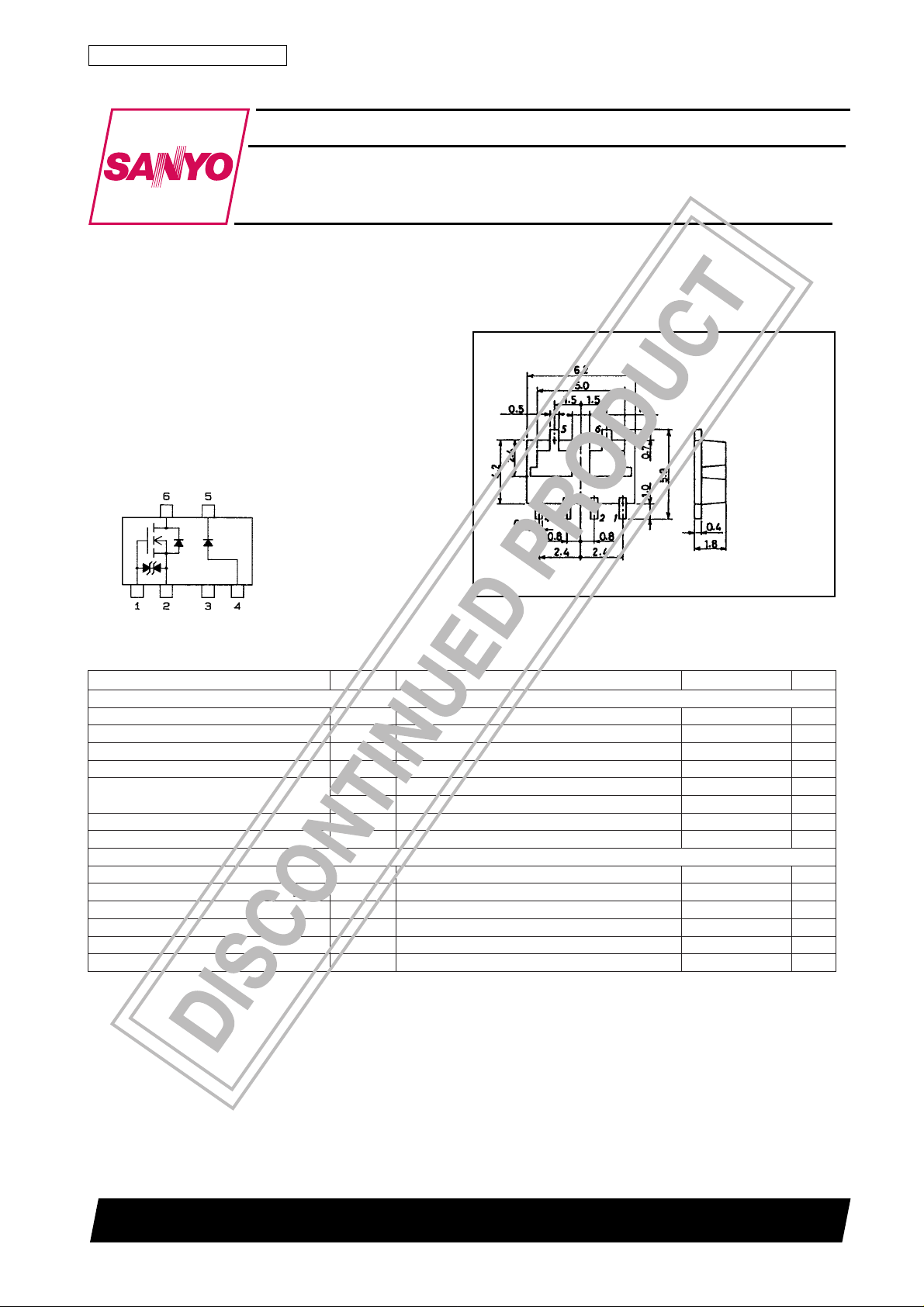
Electrical Connection
1:Gate
2:Source
3:No connection
4:Anode
5:Cathode
6:Drain
Specifications
Absolute Maximum Ratings at Ta = 25˚C
retemaraPlobmySsnoitidnoCsgnitaRtinU
]TEFSOM[
egatloVecruoS-ot-niarDV
egatloVecruoS-ot-etaGV
)CD(tnerruCniarDI
)esluP(tnerruCniarDI
noitapissiDrewoPelbawollA
erutarepmeTlennahChcT 051
erutarepmeTegarotSgtsT 051+ot55–
]DBS[
tnerruCdeifitceRegarevAI
tnerruCdrawroFegruSI
erutarepmeTnoitcnuJjT 521+ot55–
erutarepmeTegarotSgtsT 051+ot55–
· Marking:853
(Top view)
SSD
SSG
D
P
P
egatloVesreveRkaePevititepeRV
egatloVegruSesreveRkaePevititeper-noNV
O
WP ≤ elcycytud,sµ01 ≤ %18A
PD
Tc=25˚C
D
Mounted on ceramic board (750mm
D
MRR
MSR
MSF
Package Dimensions
unit:mm
2119
[FX853]
1:Gate
2:Source
3:No connection
4:Anode
5:Cathode
6:Drain
SANYO:XP6
(Bottom view)
2
×0.8mm)
elcyc1,evaweniszH05 5A
Continued on next page.
03V
51±V
2A
6W
5.1W
˚C
˚C
05V
55V
005Am
˚C
˚C
52098HA (KT)/71095TS (KOTO) TA-0118 No.4893-1/4
Page 2
FX853
Continued from preceding page.
Electrical Characteristics at Ta = 25˚C
retemaraPlobmySsnoitidnoC
]TEFSOM[
egatloVnwodkaerBS-DV
tnerruCniarDegatloVetaG-oreZI
tnerruCegakaeLecruoS-ot-etaGI
egatloVffotuCV
ecnattimdArefsnarTdrawroFY|sf|VSDI,V01=
ecnatsiseRetatS-NOecruoS-ot-niarDcitatS
R
R
ecnaticapaCtupnIssiCV
ecnaticapaCtuptuOssoCV
ecnaticapaCrefsnarTesreveRssrCV
emiTyaleDNO-nruTt
emiTesiRt
emiTyaleDFFO-nruTt
emiTllaFt
egatloVdrawroFedoiDV
]DBS[
egatloVesreveRV
egatloVdrawroFV
tnerruCesreveRI
ecnaticapaClanimretretnICV
emiTyrevoceResreveR
ecnatsiseRlamrehT
I
V,Am1=
SSD)RB(
D
V
SSD
SSG
r
f
DS
R
F
R
rrtIFI=
SD
V
SG
V
)ffo(SG
SD
I
)no(SD
D
I
)no(SD
D
SD
SD
SD
)no(d
)ffo(d
I
S
I
R
I
F
VRV52= 05Aµ
R
a-jhtR 001
R
0=03V
SG
V,V03=
0=001Aµ
SG
V,V21±=
0=01±Aµ
SD
I,V01=
Am1=0.10.2V
D
A1=2.10.2S
D
V,A1=
V01=81.052.0
SG
V,A1=
V4=52.083.0
SG
zHM1=f,V01=071Fp
zHM1=f,V01=001Fp
zHM1=f,V01=03Fp
tiucriCtseTdeificepseeS7sn
tiucriCtseTdeificepseeS11sn
tiucriCtseTdeificepseeS53sn
tiucriCtseTdeificepseeS52sn
V,A2=
0=0.1V
SG
Aµ002=05V
Am005= 55.0V
elcyCzHM1=f,V01=81Fp
sgnitaR
nimpytxam
tiucrICtseTdeificepseeS,Am001= 01sn
˚C/WMounted on ceramic board (750mm2×0.8mm)
tinU
Ω
Ω
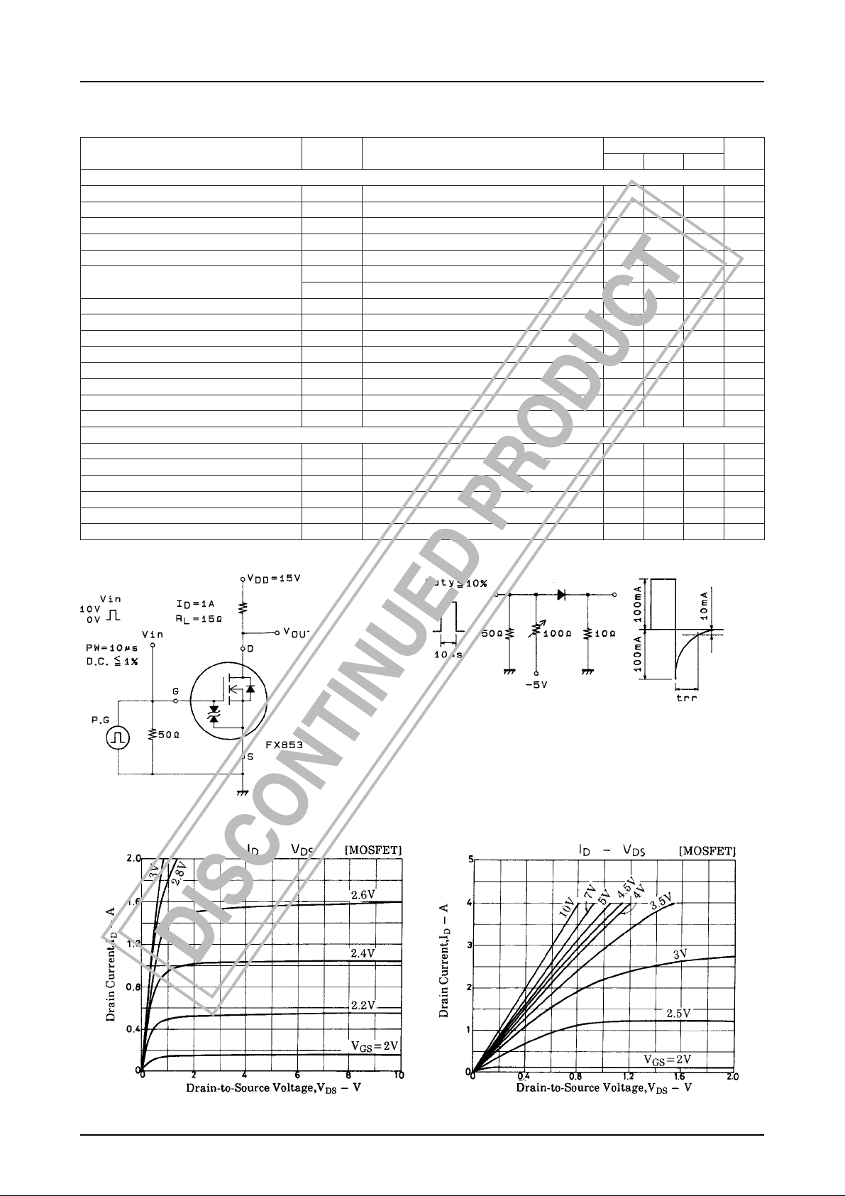
Switching Time Test CIrcuit [MOSFET]
Trr Test Circuit [SBD]
No.4893-2/4
Page 3

FX853
No.4893-3/4
Page 4

FX853
No products described or contained herein are intended for use in surgical implants, life-support systems,
aerospace equipment, nuclear power control systems, vehicles, disaster/crime-prevention equipment and
the like, the failure of which may directly or indirectly cause injury, death or property loss.
Anyone purchasing any products described or contained herein for an above-mentioned use shall:
Accept full responsibility and indemnify and defend SANYO ELECTRIC CO., LTD., its affiliates,
subsidiaries and distributors and all their officers and employees, jointly and severally, against any
and all claims and litigation and all damages, cost and expenses associated with such use:
Not impose any responsibilty for any fault or negligence which may be cited in any such claim or
litigation on SANYO ELECTRIC CO., LTD., its affiliates, subsidiaries and distributors or any of
their officers and employees jointly or severally.
Information (including circuit diagrams and circuit parameters) herein is for example only; it is not guaranteed for volume production. SANYO believes information herein is accurate and reliable, but no guarantees
are made or implied regarding its use or any infringements of intellectual property rights or other rights of
third parties.
This catalog provides information as of May, 1998. Specifications and information herein are subject to
change without notice.
PS No.4893-4/4
 Loading...