

Page 1
SANYO Electric Co.,Ltd. Semiconductor Bussiness Headquaters
TOKYO OFFICE Tokyo Bldg., 1-10, 1 Chome, Ueno, Taito-ku, TOKYO, 110-8534 JAPAN
P-Channel Silicon MOSFET
Ultrahigh-Speed Switching Applications
Ordering number:EN4888
FX605
Features
· Composite type composed of two low ON-resistance
P-channel MOSFET chips for ultrahigh-speed
switching and low-voltage drive.
· Facilitates high-density mounting.
· The FX605 is formed with two chips, each being
equivalent to the 2SJ190, placed in one package.
· Matched pair characteristics.
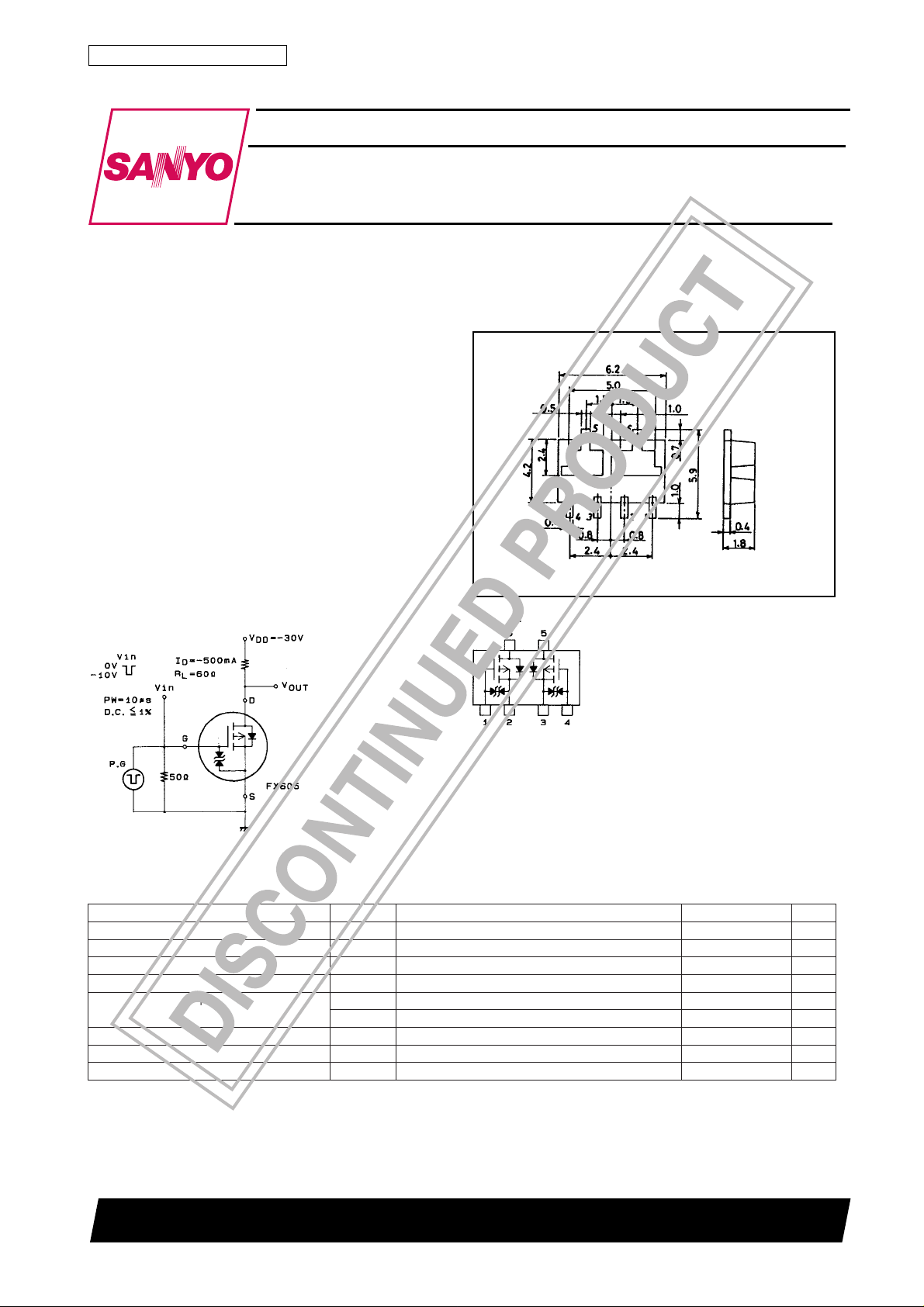
Switching Time Test CIrcuit
Package Dimensions
unit:mm
2120
[FX605]
1:Gate1
2:Source1
3:Source2
4:Gate2
5:Drain2
6:Drain1
SANYO:XP6
(Bottom view)
Electrical Connection
1:Gate1
2:Source1
3:Source2
4:Gate2
5:Drain2
6:Drain1
Specifications
Absolute Maximum Ratings at Ta = 25˚C
retemaraPlobmySsnoitidnoCsgnitaRtinU
egatloVecruoS-ot-niarDV
egatloVecruoS-ot-etaGV
)CD(tnerruCniarDI
)esluP(tnerruCniarDI
noitapissiDrewoPelbawollA
noitapissiDlatoTP
erutarepmeTlennahChcT 051
erutarepmeTegarotSgtsT 051+ot55–
· Marking:605
D
PD
P
D
P
D
T
(Top view)
SSD
SSG
WP ≤ elcycytud,sµ01 ≤ %14–A
Tc=25˚C, 1unit
Mounted on ceramic board (750mm
Mounted on ceramic board (750mm
2
×0.8mm) 1unit
2
×0.8mm)
Continued on next page.
06–V
51±V
1–A
6W
5.1W
2W
˚C
˚C
52098HA (KT)/71095MO(KOTO) TA-0111 No.4888-1/4
Page 2
Continued from preceding page.
Electrical Characteristics at Ta = 25˚C
FX605
retemaraPlobmySsnoitidnoC
egatloVnwodkaerBS-DV
tnerruCniarDegatloVetaG-oreZI
tnerruCegakaeLecruoS-ot-etaGI
egatloVffotuCV
ecnattimdArefsnarTdrawroFY|sf|VSDI,V01–=
ecnatsiseRetatS-NOecruoS-ot-niarDcitatS
R
R
ecnaticapaCtupnI
ecnaticapaCtuptuO
ecnaticapaCrefsnarTesreveR
emiTyaleDNO-nruT
emiTesiR
emiTyaleDFFO-nruT
emiTllaF
egatloVdrawroFedoiD
t
t
V
I
SSD)RB(
D
V
SSD
SSG
ssiCV
ssrCV
t
r
t
f
DS
SD
V
SG
V
)ffo(SG
SD
I
)no(SD
D
I
)no(SD
D
SD
ssoCV
SD
SD
)no(d
)ffo(d
I
S
V,Am1–=
0=06–V
SG
V,V06–=
0=001–Aµ
SG
V,21±=
0=01±Aµ
SD
I,V01–=
Am1–=0.1–0.2–V
D
D
V,Am005–=
V,Am005–=
V,A1–=
SG
Am005–=6.00.1S
V01–=9.02.1
SG
V4–=2.16.1
SG
zHM1=f,V02–=061Fp
zHM1=f,V02–=06Fp
zHM1=f,V02–=01Fp
tiucriCtseTdeificepSeeS01sn
tiucriCtseTdeificepSeeS31sn
tiucriCtseTdeificepSeeS07sn
tiucriCtseTdeificepSeeS03sn
0=9.0–V
sgnitaR
nimpytxam
tinU
Ω
Ω
No.4888-2/4
Page 3

FX605
No.4888-3/4
Page 4

FX605
No products described or contained herein are intended for use in surgical implants, life-support systems,
aerospace equipment, nuclear power control systems, vehicles, disaster/crime-prevention equipment and
the like, the failure of which may directly or indirectly cause injury, death or property loss.
Anyone purchasing any products described or contained herein for an above-mentioned use shall:
Accept full responsibility and indemnify and defend SANYO ELECTRIC CO., LTD., its affiliates,
subsidiaries and distributors and all their officers and employees, jointly and severally, against any
and all claims and litigation and all damages, cost and expenses associated with such use:
Not impose any responsibilty for any fault or negligence which may be cited in any such claim or
litigation on SANYO ELECTRIC CO., LTD., its affiliates, subsidiaries and distributors or any of
their officers and employees jointly or severally.
Information (including circuit diagrams and circuit parameters) herein is for example only; it is not guaranteed for volume production. SANYO believes information herein is accurate and reliable, but no guarantees
are made or implied regarding its use or any infringements of intellectual property rights or other rights of
third parties.
This catalog provides information as of May, 1998. Specifications and information herein are subject to
change without notice.
PS No.4888-4/4
 Loading...