

SANYO Electric Co.,Ltd. Semiconductor Bussiness Headquaters
TOKYO OFFICE Tokyo Bldg., 1-10, 1 Chome, Ueno, Taito-ku, TOKYO, 110-8534 JAPAN
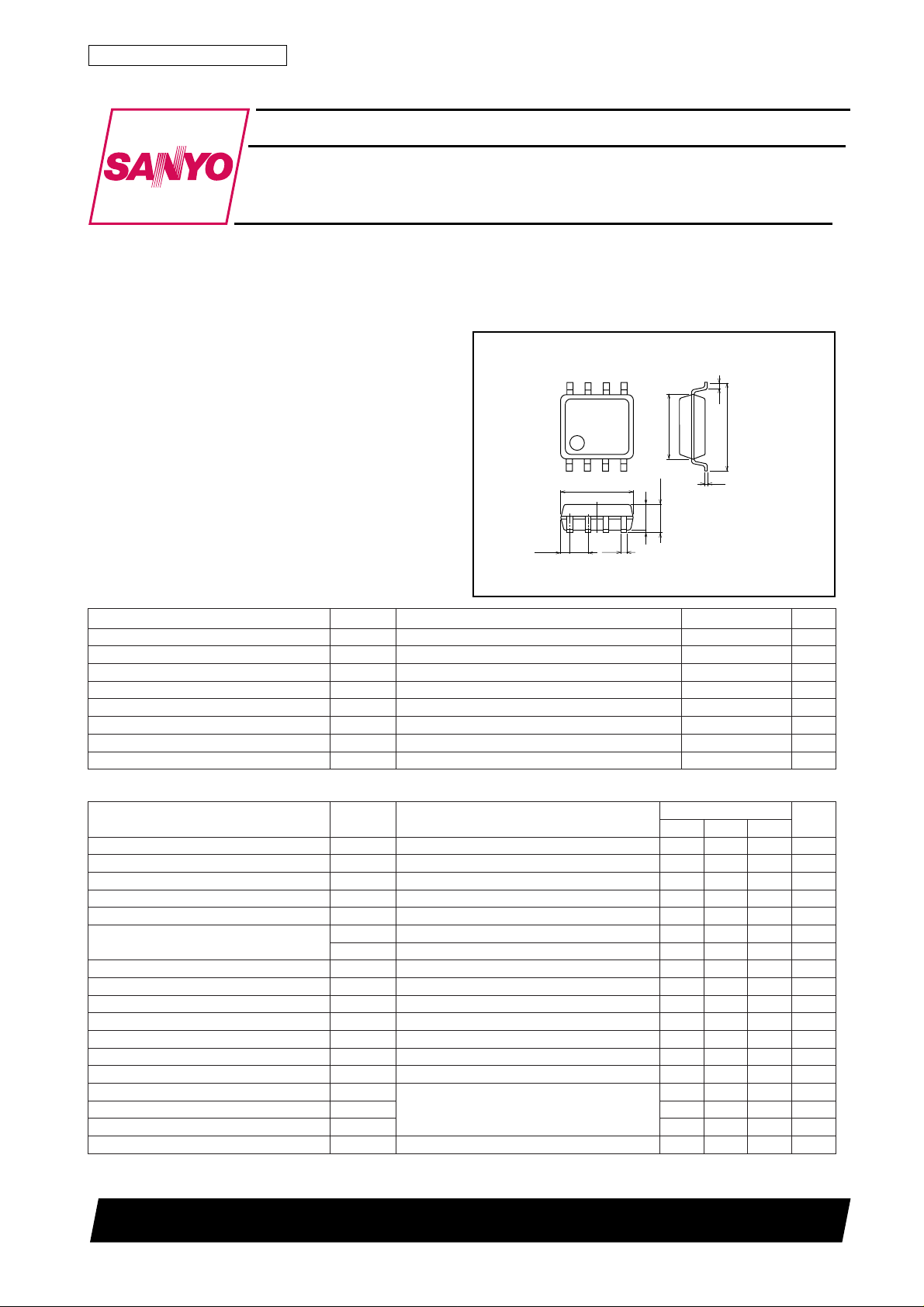
N-Channel Silicon MOSFET
DC-DC Converter Applications
Ordering number:EN5579A
FW211
Features
· Low ON resistance.
· 2.5V drive.
Specifications
Absolute Maximum Ratings at Ta = 25˚C
retemaraPlobmySsnoitidnoCsgnitaRtinU
egatloVecruoS-ot-niarDV
egatloVecruoS-ot-etaGV
)CD(tnerruCniarDI
)eslup(tnerruCniarDI
noitapissiDrewoPelbawollAP
noitapissiDlatoTP
erutarepmeTlennahChcT 051
erutarepmeTegarotSgtsT 051+ot55–
D
D
T
Package Dimensions
unit:mm
2129
[FW211]
58
4.4
14
1.27
0.595
SSD
SSG
PW≤10µs, duty cycle≤1%
PD
Mounted on a ceramic board (1000mm2×0.8mm) 1unit
Mounted on a ceramic board (1000mm2×0.8mm)
5.0
0.43
1.8max
1.5
0.1
0.3
6.0
1:Source 1
2:Gate 1
3:Source 2
0.2
4:Gate 2
5:Drain 2
6:Drain 2
7:Drain 1
8:Drain 1
SANYO:SOP8
02V
01±V
6A
25A
7.1W
0.2W
˚C
˚C
Electrical Characteristics at Ta=25˚C
retemaraPlobmySsnoitidnoC
egatloVnwodkaerBecruoS-ot-niarDV
tnerruCniarDegatloVetaGoreZI
tnerruCegakaeLecruoS-ot-etaGI
egatloVffotuCV
ecnattimdArefsnarTdrawroF|sfy|VSDI,V01=
ecnatsiseRetatS-NOecruoS-ot-niarDcitatS
R
R
ecnaticapaCtupnIssiCV
ecnaticapaCtuptuOssoCV
ecnaticapaCrefsnarTesreveRssrCV
emiTyaleDNO-nruTt
emiTesiRt
emiTyaleDFFO-nruTt
emiTllaFt
egrahCetaGlatoTgQ
egrahCecruoS-ot-etaGsgQ 5Cn
egrahC"relliM"niarD-ot-etaGdgQ 7Cn
egatloVdrawroFedoiDV
SSD
SSG
r
f
DS
SSD)RB(
)ffo(SG
1IDV,A5=
)no(SD
2IDV,A2=
)no(SD
)no(d
)ffo(d
I
V
V
V
V
I
V,Am1=
D
SD
SG
SD
SD
SD
SD
SD
S
0=02V
SG
V,V02=
0=001Aµ
SG
V,V8±=
0=01±Aµ
SD
I,V01=
Am1=4.03.1V
D
A5=951S
D
V4=7253mΩ
SG
V5.2=5384mΩ
SG
zHM1=f,V01=057Fp
zHM1=f,V01=025Fp
zHM1=f,V01=003Fp
tiucriCtseTdeificepSeeS02sn
tiucriCtseTdeificepSeeS002sn
tiucriCtseTdeificepSeeS051sn
tiucriCtseTdeificepSeeS051sn
V,V01=
V,A5=
SG
I,V01=
SG
D
0=0.12.1V
sgnitaR
nimpytxam
03Cn
A1=
tinU
61598TS (KOTO) TA-0861 No.5579-1/3
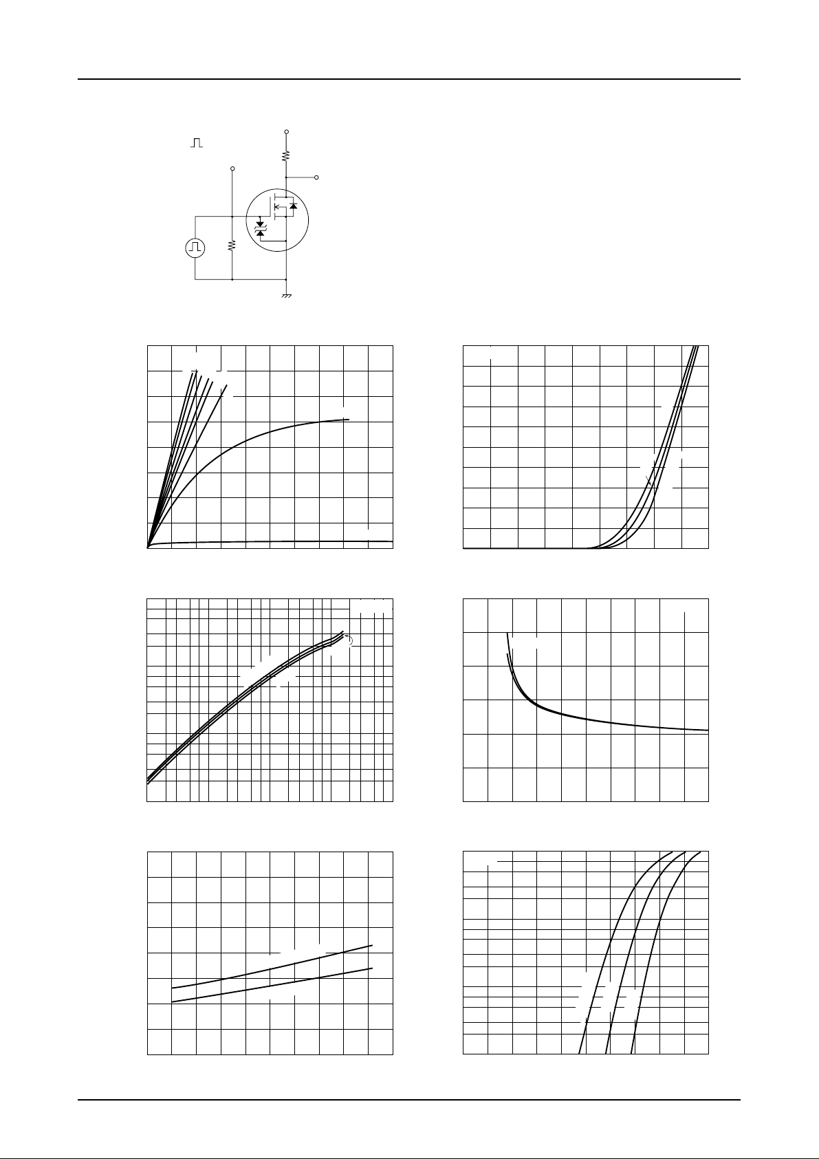
Switching Time Test Circuit
V
4V
0V
PW=10µs
D.C.≤1%
IN
V
VDD=10V
ID=5A
IN
G
RL=2Ω
D
V
FW211
OUT
–A
D
Drain Current, I
100
–S
fs |
y
|
10
1.0
8
7
6
5
4
3
2
1
0
0 0.1
7
5
3
2
7
5
3
2
7
P.G
8V
6V
4V
3V
2.5V
50Ω
ID-
2V
FW211
S
V
DS
1.5V
0.2 0.3 0.4 0.5 0.6 0.7 0.8 0.9 1.0
Drain-to-Source Voltage,VDS–V
|yfs|
Ta=
25˚C
-
-
75˚C
I
D
25˚C
VGS=1V
VDS=10V
10
–A
D
Drain Current, I
60
50
–mΩ
)
on
40
DS (
30
20
VDS=10V
9
8
7
6
5
4
3
2
1
0
0 0.2
ID-
V
GS
75˚C
25˚C
-
Ta=
0.4 0.6 0.8 1.0 1.2 1.4 1.6 1.8
Gate-to-Source Voltage, V
R
(on)
DS
-
–V
GS
V
GS
Tc=25˚C
ID=5A
2A
25˚C
Forward Transfer Admittance,
0.1
2233557
0.01
0.1
Drain Current, ID–A
80
70
–mΩ
60
)
on
50
DS (
40
30
20
10
Static Drain-to-Source
ON-State Resistance, R
0
-60 -40
-20 0 20 40 60 80 100 120 140
Case Temperature, Tc – ˚C
2357
R
(on)
DS
I
D
I
D
23 57102357
1.0
-
Tc
=2.5V
GS
=2A,V
=4V
GS
=5A,V
Static Drain-to-Source
100
10
ON-State Resistance, R
0
01
10
VGS=0
7
5
3
2
–A
1.0
F
7
5
3
2
0.1
7
Forward Current, I
5
3
2
0.01
0 0.1 0.2 0.3 0.4 0.5 0.6 0.7 0.8 0.9 1.0
2345678910
Gate-to-Source Voltage, V
IF-
V
Ta=75˚C
Diode Forward Voltage, V
SD
25˚C
GS
SD
25˚C
-
–V
–V
No.5579-2/3
 Loading...