

SANYO FW133 Datasheet
Ordering number : ENN6784
FW133
P-Channel Silicon MOSFET
FW133
Load Switching Applications
Features
•
4V drive.
• Low ON-resistance.
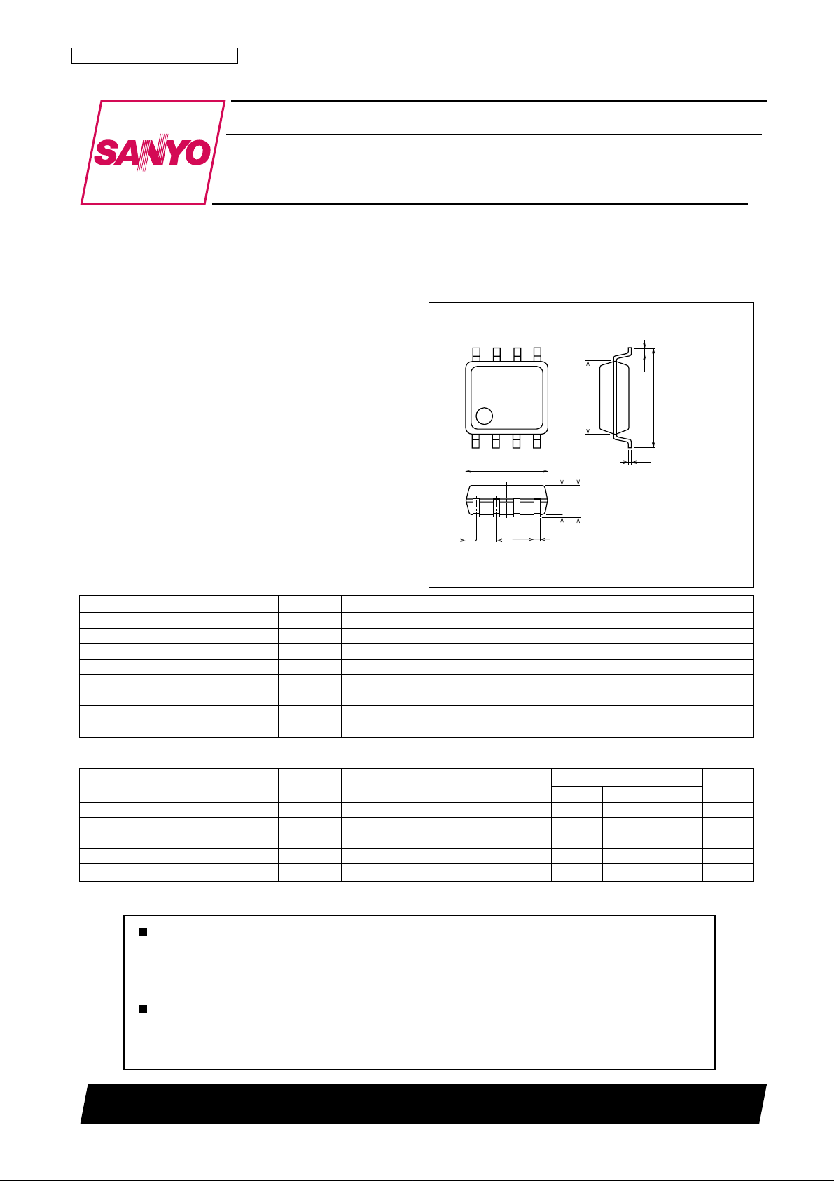
Package Dimensions
unit : mm
2129
[FW133]
58
0.3
4.4
6.0
1 : Source1
14
5.0
1.8max
1.5
0.2
2 : Gate1
3 : Source2
4 : Gate2
5 : Drain2
6 : Drain2
7 : Drain1
8 : Drain1
SANYO : SOP8
Specifications
0.595
1.27
0.43
0.1
Absolute Maximum Ratings at Ta=25°C
Parameter Symbol Conditions Ratings Unit
Drain-to-Source Voltage V
Gate-to-Source Voltage V
Drain Current (DC) I
Drain Current (Pulse) I
Allowable Power Dissipation P
Total Dissipation P
Channel T emperature T ch 150 °C
Storage T emperature Tstg --55 to +150 °C
DSS
GSS
D
DP
D
T
PW≤10µs, duty cycle≤1% --32 A
Mounted on a ceramic board (1000mm2✕0.8mm) 1unit
Mounted on a ceramic board (1000mm2✕0.8mm)
--30 V
±20 V
--7 A
1.7 W
2.0 W
Electrical Characteristics at T a=25 °C
Parameter Symbol Conditions
Drain-to-Source Breakdown Voltage V
Zero-Gate Voltage Drain Current I
Gate-to-Source Leakage Current I
Cutoff Voltage VGS(off) VDS=--10V, ID=--1mA --1.0 --2.4 V
Forward Transfer Admittance
(BR)DSSID
DSS
GSS
yfs
=--1mA, VGS=0 --30 V
VDS=--30V, VGS=0 --1 µA
VGS=±16V, VDS=0 ±10 µA
VDS=--10V, ID=--7A 8.4 12 S
Marking : W133 Continued on next page.
Any and all SANYO products described or contained herein do not have specifications that can handle
applications that require extremely high levels of reliability, such as life-support systems, aircraft's
control systems, or other applications whose failure can be reasonably expected to result in serious
physical and/or material damage. Consult with your SANYO representative nearest you before using
any SANYO products described or contained herein in such applications.
SANYO assumes no responsibility for equipment failures that result from using products at values that
exceed, even momentarily, rated values (such as maximum ratings, operating condition ranges, or other
parameters) listed in products specifications of any and all SANYO products described or contained
herein.
Ratings
min typ max
Unit
SANYO Electric Co.,Ltd. Semiconductor Company
TOKYO OFFICE Tokyo Bldg., 1-10, 1 Chome, Ueno, Taito-ku, TOKYO, 110-8534 JAPAN
N1500 TS IM TA-2298
No.6784-1/4
FW133
Continued from preceding page.
Parameter Symbol Conditions
RDS(on)1 ID=--7A, VGS=--10V 24 32 mΩ
Static Drain-to-Source On-State Resistance
Input Capacitance Ciss VDS=--10V, f=1MHz 1700 pF
Output Capacitance Coss VDS=--10V, f=1MHz 380 pF
Reverse Transfer Capacitance Crss VDS=--10V, f=1MHz 240 pF
Turn-ON Delay Time td(on) See specified Test Circuit 15 ns
Rise Time t
Turn-OFF Delay Time td(off) See specified Test Circuit 85 ns
Fall Time t
Total Gate Charge Qg VDS=--10V, VGS=--10V, ID=--7A 32 nC
Gate-to-Source Charge Qgs VDS=--10V, VGS=--10V, ID=--7A 4.5 nC
Gate-to-Drain “Miller” Charge Qgd VDS=--10V, VGS=--10V, ID=--7A 5 nC
Diode Forward Voltage V
RDS(on)2 ID=--4A, VGS=--4.5V 36 51 mΩ
RDS(on)3 ID=--4A, VGS=--4V 40 56 mΩ
See specified Test Circuit 150 ns
r
See specified Test Circuit 90 ns
f
SD
IS=--7A, VGS=0 --1.0 --1.5 V
min typ max
Switching Time Test Circuit
VDD= --15V
V
IN
0V
--10V
PW=10µs
D.C.≤1%
V
IN
G
D
ID= --7A
RL=2.1Ω
V
OUT
Ratings
Unit
P.G
--10
--6.0V
--4.5V
--8
-- A
D
--6
--4
--10.0V
I
D
--4.0V
50Ω
-- V
--3.0V
DS
S
V
GS
Drain Current, I
--2
0
0 --0.1 --0.2 --0.3 --0.4 --0.5 --0.6 --0.7 --0.8 --0.9 --1.0
Drain-to-Source V oltage, V
DS
-- V
FW133
= --2.5V
IT02582
--12
VDS= --10V
--10
--8
-- A
D
--6
--4
Drain Current, I
--2
0
0
I
-- V
D
GS
Gate-to-Source V oltage, V
Ta=75°C
25°C
--25°C
--3.0
--2.5--1.5 --2.0--1.0--0.5 --3.5
GS
-- V
IT02583
No.6784-2/4
 Loading...