

SANYO FW113 Datasheet
FW113
Ordering number :EN5847
S/W Load Applications
SANYO Electric Co.,Ltd. Semiconductor Bussiness Headquarters
TOKYO OFFICE Tokyo Bldg., 1-10, 1 Chome, Ueno, Taito-ku, TOKYO, 110-8534 JAPAN
P-Channel Silicon MOS FET
Features
· 4V drive.
· Low ON resistance.
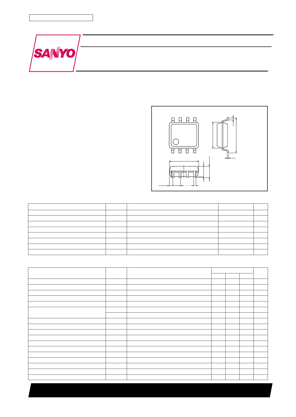
Package Dimensions
unit:mm
2129
[FW113]
58
0.3
Specifications
Absolute Maximum Ratings at Ta = 25˚C
retemaraPlobmySsnoitidnoCsgnitaRtinU
egatloVecruoS-ot-niarDV
egatloVecruoS-ot-etaGV
)CD(tnerruCniarDI
)eslup(tnerruCniarDI
noitapissiDrewoPelbawollAP
noitapissiDlatoTP
erutarepmeTlennahChcT 051
erutarepmeTegarotSgtsT 051+ot55–
Electrical Characteristics at Ta = 25˚C
retemaraPlobmySsnoitidnoC
egatloVnwodkaerBS-DV
tnerruCniarDegatloVetaGoreZI
tnerruCegakaeLecruoS-ot-etaG
tnerruCffotuCV
ecnattimdArefsnarTdrawroF|sfy|VSDI,V01–=
ecnatsiseRetatS-NOecruoS-ot-niarDcitatS
ecnaticapaCtupnIssiC
ecnaticapaCtuptuO
ecnaticapaCrefsnarTesreveR
emiTyaleDNO-nruT
emiTesiR
emiTyaleDFFO-nruT
emiTllaF
egrahCetaGlatoT
egrahCecruoS-ot-etaG
egrahC)"relliM"(niarD-ot-etaG
egatloVdrawroFedoiD
D
D
T
I
R
R
t
t
r
t
t
f
V
4.4
1:Source1
6.0
2:Gate1
3:Source2
14
5.0
1.8max
1.5
0.2
4:Gate2
5:Drain2
6:Drain2
7:Drain1
8:Drain1
1.27
0.595
SSD
SSG
WP ≤ elcycytud,sµ01 ≤ %123–A
PD
Mounted on ceramic board (1000mm2×0.8mm) 1unit
Mounted on ceramic board (1000mm
I
SSD)RB(
D
V
SSD
V
SSG
V
)ffo(SG
1IDV,A5–=
)no(SD
2IDV,A2–=
)no(SD
V
ssoCV
ssrCV
)no(d
)ffo(d
gQVSDV,V01–=
sgQVSDV,V01–=
dgQVSDV,V01–=
I
DS
S
V,Am1–=
0=03–V
SG
V,V03–=
SD
SG
SD
SD
SD
SD
V,A5–=
0=001–Aµ
SG
V,V61±=
0=01±Aµ
SD
I,V01–=
Am1–=0.1–5.2–V
D
A5–=58S
D
V01–=2435mΩ
SG
V4–=58021mΩ
SG
zHM1=f,V01–=028
zHM1=f,V01–=074Fp
zHM1=f,V01–=032Fp
tiucriCtseTdeificepseeS51sn
tiucriCtseTdeificepseeS051sn
tiucriCtseTdeificepseeS58sn
tiucriCtseTdeificepseeS09sn
I,V01–=
SG
SG
SG
0=0.1–5.1–V
SG
D
I,V01–=
D
I,V01–=
D
0.43
2
×0.8mm)
A5–=52Cn
A5–=5Cn
A5–=7Cn
0.1
SANYO:SOP8
sgnitaR
nimpytxam
03–V
02±V
5–A
7.1W
0.2W
˚C
˚C
tinU
Fp
52698TS (KOTO) TA-1215 No.5847-1/3
Switching Time Test Circuit
=
V
–15V
DD
=
I
–5A
D
=
R
3Ω
L
D
–10V
V
0V
PW=10µs
D.C.≤1%
IN
V
IN
FW113
V
OUT
P.G
A
-
D
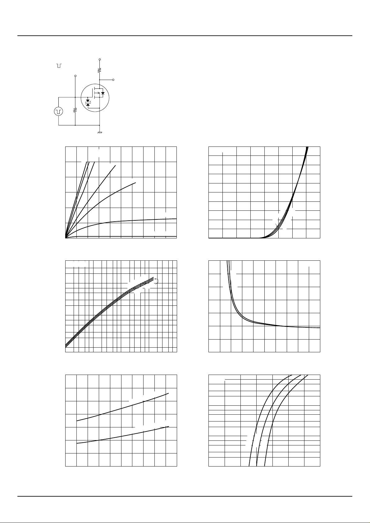
Drain Current, I
|-S
fs
y
10
1.0
-6
-5
-4
-3
-2
-1
0
0-0.1
5
VDS=–10V
3
2
7
5
3
2
7
G
50Ω
–8.0V
–10.0V
-0.2 -0.3 -0.4 -0.5 -0.6 -0.7 -0.8 -0.9 -1.0 0 -0.5
Drain-to-Source Voltage, V
S
–6.0V
ID-
–4.0V
y
|
FW113
fs
V
–3.5V
|-I
DS
DS
D
Ta=–25˚C
75˚C
-10
-9
-8
A
-7
-
-6
D
-5
-4
–3.0V
=–
V
2.5V
GS
-3
Drain Current, I
-2
-1
0
- V Gate-to-Source Voltage, VDS-V
140
120
–mΩ
)
25˚C
100
on
DS (
80
60
40
VDS=–10V
=–2A
ID-
V
GS
75˚C
25˚C
Ta=–25˚C
-1.0 -1.5 -2.0 -2.5 -3.0 -4.0-3.5
R
(on)
-
DS
=–5A
D
D
I
I
V
GS
Tc=25˚C
Forwaard Transfer Addmittance,|
0.1
7
-0.01
2233557
-0.1
2357
Drain Current, ID-A
R
140
120
–mΩ
)
100
on
DS (
80
60
40
20
Static Drain-to-Source
ON-State Resistance, R
0
-60 -40
-20 0 20 40 60 80 100 120 140
DS
Case Temperature, Tc - ˚C
(on)
-1.0
2357
-
Tc
=–2A
I
D
=–5A,V
I
D
-10
,V
2357
=–4V
GS
=–10V
GS
-100
20
Static Drain-to-Source
ON-State Resistance, R
0
0-2
-4 -6 -8 -10 -12 -14 -16 -18 -20
Gate-to-Source Voltage,V
-10
VGS=0
7
5
3
2
-A
-1.0
F
7
5
3
2
-0.1
7
Forward Current, I
5
3
2
-0.01
0 -0.2 -0.4 -0.6 -0.8 -1.4-1.2-1.0
IF-
25˚C
Ta=75˚C
Diode Forward Voltage, VSD–V
25˚C
–
- V
GS
V
SD
No.5847-2/3
 Loading...