

SANYO FSS216 Datasheet
Any and all SANYO products described or contained herein do not have specifications that can handle
applications that require extremely high levels of reliability, such as life-support systems, aircraft’s
control systems, or other applications whose failure can be reasonably expected to result in serious
physical and/or material damage. Consult with your SANYO representative nearest you before using
any SANYO products described or contained herein in such applications.
SANYO assumes no responsibility for equipment failures that result from using products at values that
exceed, even momentarily, rated values (such as maximum ratings, operating condition ranges,or other
parameters) listed in products specifications of any and all SANYO products described or contained
herein.
N-Channel Silicon MOSFET
DC/DC Converter Applications
Ordering number:ENN5934A
FSS216
SANYO Electric Co.,Ltd. Semiconductor Company
TOKYO OFFICE Tokyo Bldg., 1-10, 1 Chome, Ueno, Taito-ku, TOKYO, 110-8534 JAPAN
Features
· Low ON-resistance.
· 4V drive.
Specifications
Absolute Maximum Ratings at Ta = 25˚C
retemaraPlobmySsnoitidnoCsgnitaRtinU
egatloVecruoS-ot-niarDV
egatloVecruoS-ot-etaGV
)CD(tnerruCniarDI
)eslup(tnerruCniarDI
noitapissiDrewoPelbawollAP
erutarepmeTlennahChcT 051
erutarepmeTegarotSgtsT 051+ot55–
Electrical Characteristics at Ta = 25˚C
retemaraPlobmySsnoitidnoC
egatloVnwodkaerBecruoS-ot-niarDV
tnerruCniarDegatloVetaG-oreZI
tnerruCegakaeLecruoS-ot-etaGI
egatloVffotuCV
ecnattimdArefsnarTdrawroF|sfy|VSDI,V01=
ecnatsiseRetatS-nOecruoS-ot-niarDcitatS
ecnaticapaCtupnIssiCV
ecnaticapaCtuptuOssoCV
ecnaticapaCrefsnarTesreveRssrCV
Marking : S216
D
D
R
R
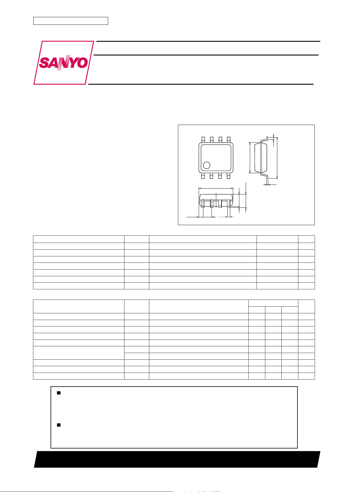
Package Dimensions
unit:mm
2116
[FSS216]
58
0.3
4.4
14
5.0
1.8max
1.5
1.27
0.595
SSD
SSG
WP ≤ elcycytud,sµ01 ≤ %125A
PD
Mounted on a ceramic board (1000mm2×0.8mm)
I
V,Am1=
0=03V
SG
V,V03=
0=01Aµ
SG
V,V61±=
0=01±Aµ
SD
I,V01=
Am1=0.14.2V
D
A01=0141S
D
V01=1151mΩ
SG
V4=0282mΩ
SG
zHM1=f,V01=0021Fp
zHM1=f,V01=007Fp
zHM1=f,V01=082Fp
SSD
SSG
)ffo(SG
1IDV,A01=
)no(SD
2IDV,A4=
)no(SD
SSD)RB(
D
V
SD
V
SG
V
SD
SD
SD
SD
0.43
0.1
nimpytxam
6.0
1 : Source
2 : Source
3 : Source
0.2
4 : Gate
5 : Drain
6 : Drain
7 : Drain
8 : Drain
SANYO : SOP8
sgnitaR
Continued on next page.
03V
42±V
01A
0.2W
˚C
˚C
tinU
71000TS (KOTO) TA-2143 No.5934-1/4
FSS216
Continued from preceding page.
retemaraPlobmySsnoitidnoC
emiTyaleDNO-nruTt
emiTesiRt
emiTyaleDFFO-nruTt
emiTllaFt
egrahCetaGlatoTgQVSDV,V01=
egrahCecruoS-ot-etaGsgQVSDV,V01=
egrahC"relliM"niarD-ot-etaGdgQVSDV,V01=
egatloVdrawroFedoiDV
)no(d
r
)ffo(d
f
SG
SG
I
DS
S
SG
V,A01=
0=8.02.1V
SG
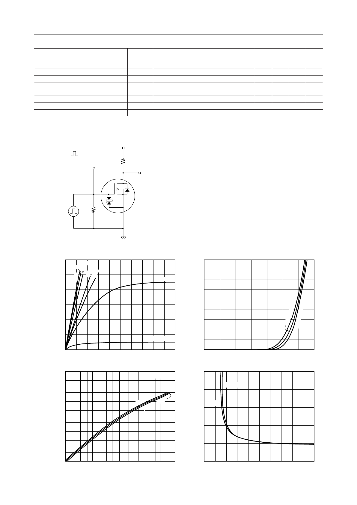
Switching Time Test Circuit
tiucriCtseTdeificepseeS51sn
tiucriCtseTdeificepseeS002sn
tiucriCtseTdeificepseeS051sn
tiucriCtseTdeificepseeS051sn
I,V01=
D
I,V01=
D
I,V01=
D
sgnitaR
nimpytxam
A01=83Cn
A01=5Cn
A01=8Cn
tinU
P.G
12
10
–A
D
Drain Current, I
100
fs|–S
y
10
1.0
Forward Transfer Admittance, |
0.1
ID-
VDD=15V
D
S
V
ID=10A
RL=1.5Ω
FSS216
DS
V
OUT
V
IN
10V
0V
V
IN
PW=10µs
D.C.≤1%
G
50Ω
6.0V
8.0V
4.0V
3.5V
10V
8
6
4
2
0
0
0.1 0.2 0.3 0.4 0.5 0.6 0.7 0.8 0.9 1.0
Drain-to-Source Voltage, VDS–V
y
|
fs
|
-
I
D
7
5
3
2
7
5
3
2
7
5
3
2
0.01
23 57
23 57
0.1
Drain Current, ID–A
1.0
°C
25
-
Ta=
°C
75
23 2357
3.0V
=2.5V
V
GS
VDS=10V
°C
25
10
ID-
V
18
VDS=10V
16
14
–A
12
D
10
8
6
Drain Current, I
4
2
0
0 0.5 1.0 1.5 2.0 2.5 3.0 3.5
GS
°C
25
Gate-to-Source Voltage, VGS–V
R
I
D
DS(on)
=10A
50
40
–mΩ
I
=4A
D
30
DS(on)
20
10
Static Drain-to-Source
On-State Resistance, R
0
0 2 4 6 8 101214161820
-
V
GS
Gate-to-Source Voltage, VGS–V
°C
75
-
Ta=
Ta=25°C
°C
25
No.5934-2/4
 Loading...