

Any and all SANYO products described or contained herein do not have specifications that can handle
applications that require extremely high levels of reliability, such as life-support systems, aircraft’s
control systems, or other applications whose failure can be reasonably expected to result in serious
physical and/or material damage. Consult with your SANYO representative nearest you before using
any SANYO products described or contained herein in such applications.
SANYO assumes no responsibility for equipment failures that result from using products at values that
exceed, even momentarily, rated values (such as maximum ratings, operating condition ranges,or other
parameters) listed in products specifications of any and all SANYO products described or contained
herein.
PNP/NPN Epitaxial Planar Silicon Transistors
Push-Pull Circuit Applications
Ordering number:ENN6457
FP207
SANYO Electric Co.,Ltd. Semiconductor Company
TOKYO OFFICE Tokyo Bldg., 1-10, 1 Chome, Ueno, Taito-ku, TOKYO, 110-8534 JAPAN
Features
· Composite type with a PNP transistor and an NPN
transistor contained in one package, facilitating highdensity mounting.
· Each device incorporated in the FP207 is equivalent
to the 2A1729 and to the 2SC4520, respectively.
Specifications
( ) : PNP
Absolute Maximum Ratings at Ta = 25˚C
retemaraPlobmySsnoitidnoCsgnitaRtinU
egatloVesaB-ot-rotcelloCV
egatloVrettimE-ot-rotcelloCV
egatloVesaB-ot-rettimEV
tnerruCrotcelloCI
)esluP(tnerruCrotcelloCI
tnerruCesaBI
noitapissiDrotcelloCP
noitapissiDrewoPlatoTP
erutarepmeTnoitcnuJjT 051
erutarepmeTegarotSgtsT 051+ot55–
OBC
OEC
OBE
C
PC
B
C
T
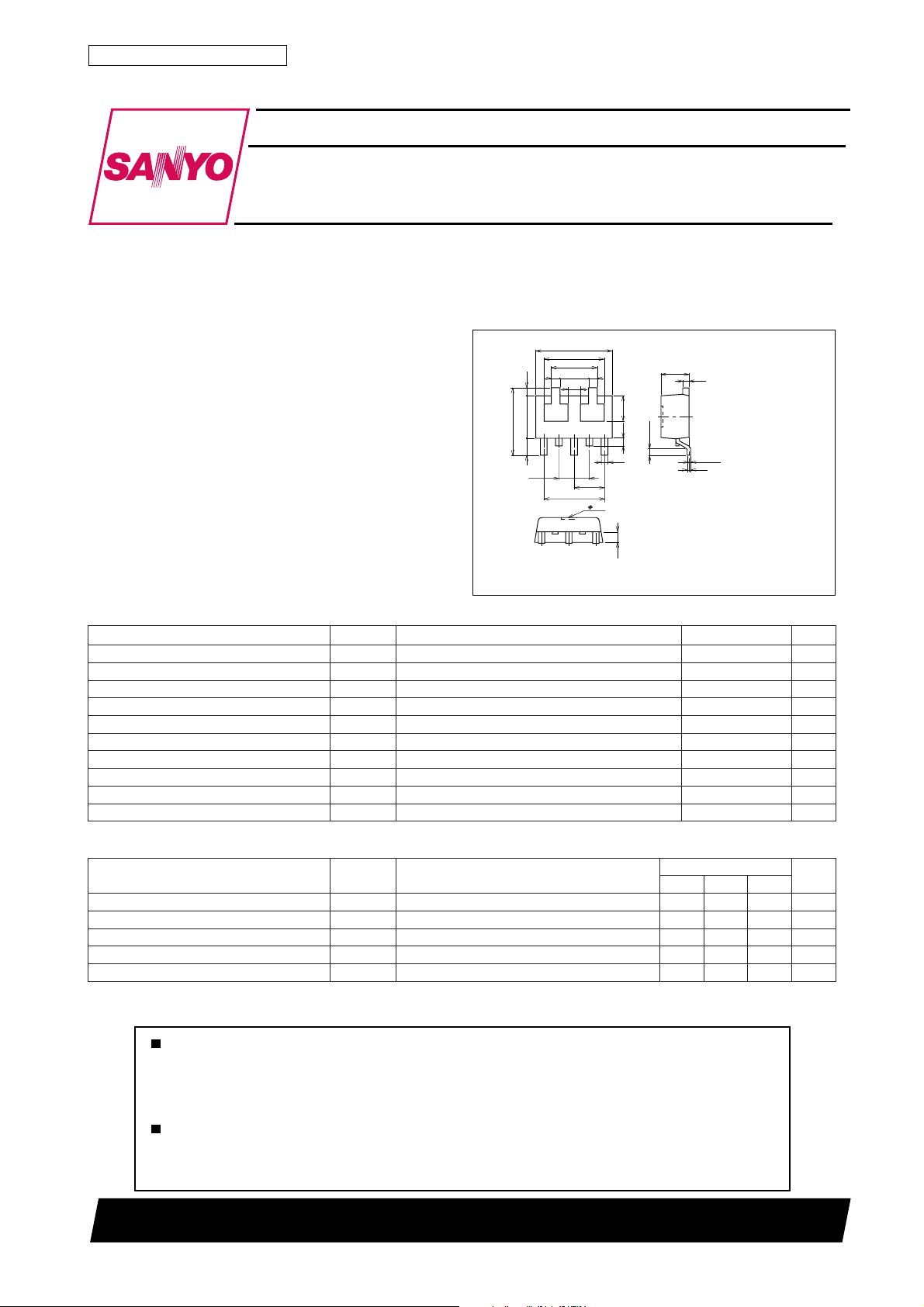
Package Dimensions
unit:mm
2097B
4.5
3.4
2.8
0.5
1.8
0.5
6
1.0
2.5
4.25max
1.0
4
2
5
3
1.75
Mounted on a ceramic board (250mm2×0.8mm) 1unit
Mounted on a ceramic board (250mm2×0.8mm)
1.75
3.5
[FP207]
0.5
7
1.57
0.5
1
0.3
1.2
0.7
1.5
0.4
0.2min
0 to 0.1
0.2
1 : Base 1 (PNP TR)
2 : Collector 1 (PNP TR)
3 : Emitter Common
4 : Collector 2 (NPN TR)
5 : Base 2 (NPN TR)
6 : Collector 2 (NPN TR)
7 : Collector 1 (PNP TR)
SANYO : PCP5 (Top view)
05)–(V
04)–(V
5)–(V
5.1)–(A
3)–(A
003Am
8.0W
1.1W
˚C
˚C
Electrical Characteristics at Ta = 25˚C
retemaraPlobmySsnotidnoC
tnerruCffotuCrotcelloCI
tnerruCffotuCrettimEI
niaGtnerruCCDh
tcudorPhtdiwdnaB-niaGf
ecnaticapaCtuptuOboCV
V
OBC
OBE
EF
T
BC
V
BE
V
EC
V
EC
BC
I,V04)–(=
0=1)–(Aµ
E
I,V3)–(=
0=1)–(Aµ
C
I,V2)–(=
C
I,V2)–(=
C
Am001)–(=001004
Am001)–(=003zHM
zHM1=f,V01)–(=31)81(Fp
nimpytxam
Marking : 207 Continued on next page.
92500TS (KOTO) TA-2925 No.6457–1/5
sgnitaR
tinU
FP207
Continued from preceding page.
retemaraPlobmySsnotidnoC
egatloVnoitarutaSrettimE-ot-rotcelloCV
egatloVnoitarutaSrettimE-ot-esaBV
egatloVnwodkaerBesaB-ot-rotcelloCV
egatloVnwodkaerBrettimE-ot-rotcelloCV
egatloVnwodkaerBesaB-ot-rettimEV
emiTNO-nruTt
emiTegarotSt
emiTllaFt
Electrical Connection (Top view) Switching Time Test Circuit
C1 C2
C1 C2
B1 EC B2
EC
EB
no
gts
f
)tas(I
C
)tas(I
C
I
OBC)RB(
C
I
OEC)RB(
C
I
OBE)RB(
E
PW=20µs
D.C.≤1%
I,Am008)–(=
B
I,Am008)–(=
B
I,Aµ01)–(=
E
R,Am1)–(=
EB
I,Aµ01)–(=
C
INPUT
Am04)–(=
Am04)–(=9.0)–(3.1)–(V
0=05)–(V
=∞ 04)–(V
0=5)–(V
tiucriCtseTdeificepseeS
tiucriCtseTdeificepseeS
tiucriCtseTdeificepseeS03)03(08)08(sn
I
B1
I
B2
R
B
V
R
50Ω
(For PNP, the polarity is reversed.)
10IB1= --10IB2= IC=400mA
+
100µF 470µF
+
VCC=25VVBE=--5V
OUTPUT
R
L
sgnitaR
nimpytxam
)3.0–()8.0–(Vm
52.07.0Vm
)05()001(sn
05001sn
)021()022(sn
051072sn
tinU
--1 .0
--0 .8
–A
C
--0 .6
C
--8mA
CE
--7mA
--6mA
--5mA
--4mA
I
-- V
--3mA
--0 .4
--2mA
Collector Current, I
--0 .2
0
0 --1 --2 --3 --4 --5
--1mA
I
B
Collector-to-Emitter Voltage, VCE–V
--1 .6
--1 .4
--1 .2
–A
C
--1 .0
--0 .8
--0 .6
--0 .4
Collector Current, I
--0 .2
IC -- V
VCE= --2V
BE
°C
Ta=75
25°C
°C
--25
[PNP] [NPN]
1.0
I
C
-- V
CE
4.0mA
3.5mA
0.8
–A
C
0.6
3.0mA
2.5mA
2.0mA
25°C
1.5mA
1.0mA
0.5mA
IB=0
°C
--25
0.4
Collector Current, I
0.2
=0
IT01846
[PNP] [NPN]
0
012345
Collector-to-Emitter Voltage, VCE–V
1.6
1.4
1.2
–A
C
1.0
0.8
0.6
0.4
Collector Current, I
0.2
IC -- V
VCE=2V
BE
Ta=75°C
IT01847
0
0 --0.2 --0.4 --0.6 --0.8 --1.2--1.0
Base-to-Emitter Voltage, VBE–V
0
0 0.2 0.4 0.6 0.8 1.21.0
IT01848 IT01849
Base-to-Emitter Voltage, VBE–V
No.6457–2/5
 Loading...