

SANYO Electric Co.,Ltd. Semiconductor Bussiness Headquaters
TOKYO OFFICE Tokyo Bldg., 1-10, 1 Chome, Ueno, Taito-ku, TOKYO, 110-8534 JAPAN
PNP Epitaxial Planar Silicon Transistor/
Composite Schottky Barrier Diode
DC-DC Converter Applications
Ordering number:EN3961A
FP102
Features
· Composite type with a PNP transistor and a Shottky
barrier diode contained in one package, facilitating
high-density mounting.
· The FP102 is formed with 2chips, one being equivalent to the 2SB1396 and the other the SB07-03C,
placed in one package.
Specifications
Absolute Maximum Ratings at Ta = 25˚C
retemaraPlobmySsnoitidnoCsgnitaRtinU
]RT[
egatloVesaB-ot-rotcelloCV
egatloVrettimE-ot-rotcelloCV
egatloVesaB-ot-rettimEV
tnerruCrotcelloCI
)esluP(tnerruCrotcelloCI
tnerruCesaBI
noitapissiDrotcelloCP
erutarepmeTnoitcnuJjT 051
]DBS[
egatloVesreveRkaePevititepeRV
egatloVegruSesreveRkaePevititeper-noNV
tnerruCdeifitceRegarevAI
tnerruCdrawroFegruSI
erutarepmeTnoitcnuJjT 521+ot55–
erutarepmeTegarotSgtsT 521+ot55–
Marking:102
Electrical Connection
OBC
OEC
OBE
C
PC
B
Mounted on ceramic board (250mm2×0.8mm)
C
MRR
MSR
O
MSF
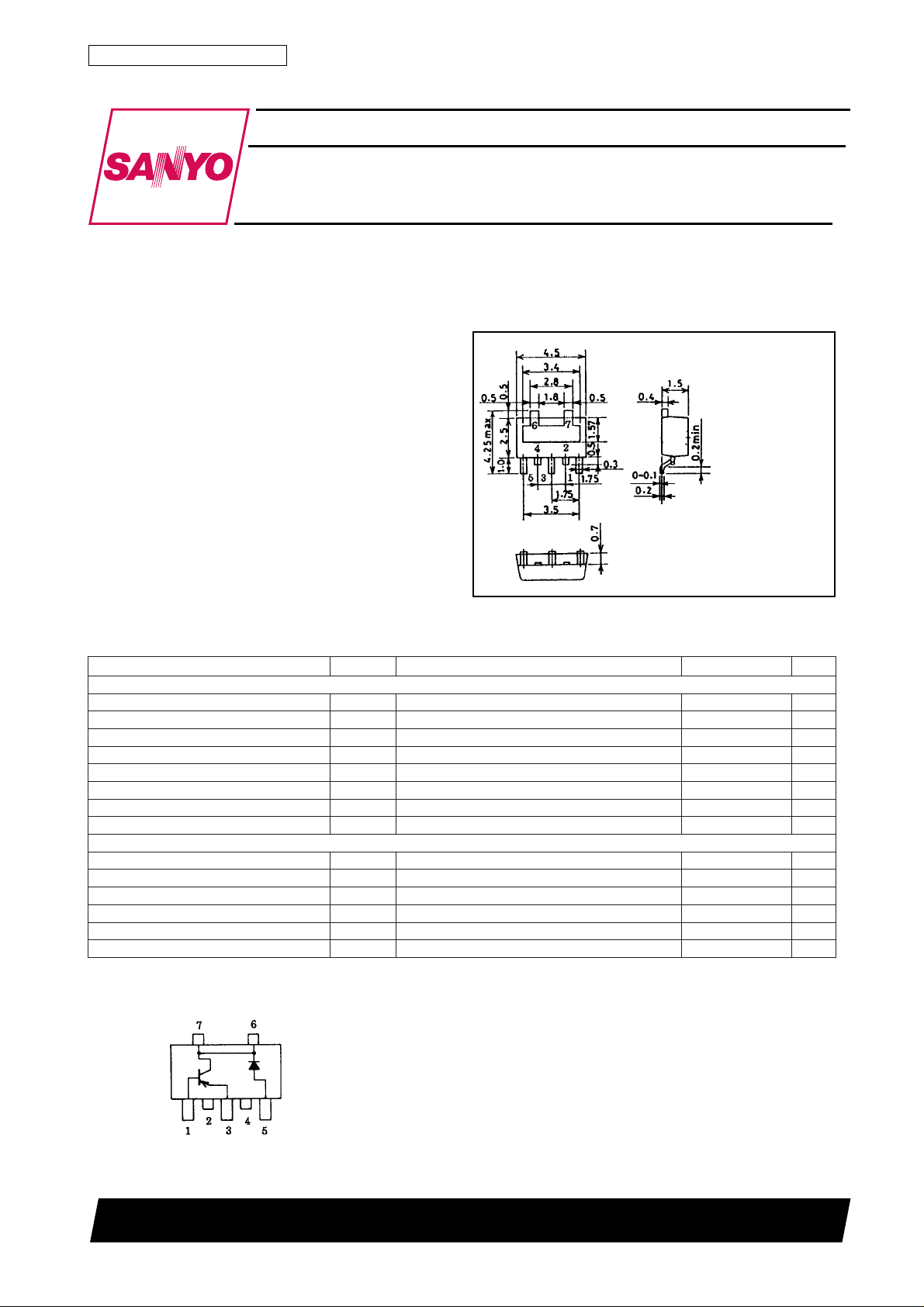
Package Dimensions
unit:mm
2088A
[FP102]
1:Base
2:Common
3:Emitter
4:Common
5:Anode
6:Common
7:Common
(Common:Collcector,
Cathode)
SANYO:PCP4
(Bottom view)
51–V
11–V
7–V
3–A
5–A
006–Am
3.1W
˚C
03V
53V
007Am
elcyc1,evaweniszH05 5A
˚C
˚C
Continued on next page.
1:Base
2:Common
3:Emitter
4:Common
5:Anode
6:Common
7:Common
(Common:Collcector, Cathode)
(Top view)
52098HA (KT)/62094MT (KOTO) AX-8060 No.3961-1/4
FP102
Continued from preceding page.
Electrical Characteristics at Ta=25˚C
retemaraPlobmySsnotidnoC
]RT[
tnerruCffotuCrotcelloCI
tnerruCffotuCrettimEI
niaGtnerruCCD
tcudorPhtdiwdnaB-niaGf
ecnaticapaCtuptuOboCV
egatloVnoitarutaSE-CV
egatloVnoitarutaSE-BV
egatloVnwodkaerBB-CV
egatloVnwodkaerBE-CV
egatloVnwodkaerBB-EV
emiTNO-nruTt
emiTegarotSgtsttiucriCtseTdeificepseeS002sn
emiTllaFt
]DBS[
egatloVesreveRV
egatloVdrawroFV
tnerruCesreveRI
ecnaticapaClanimretretnICV
emiTyrevoceResreveRt
ecnatsiseRlamrehTa-jhtR 021
hEF1VECI,V2–=
hEF2VECI,V2–=
V
OBC
V
OBE
V
T
I
)tas(EC
C
I
)tas(EB
C
I
OBC)RB(
C
I
OEC)RB(
C
I
OBE)RB(
E
no
f
I
R
R
I
F
F
VRV51= 08Aµ
R
R
IFI=
rr
Mounted on ceramic board (250mm2×0.8mm)
I,V21–=
BC
BE
EC
BC
R
0=1.0–Aµ
E
I,V6–=
0=1.0–Aµ
C
A5.0–=041065
C
A3–=07
C
I,V2–=
A3.0–=004zHM
C
zHM1=f,V01–=62Fp
I,A5.1–=
Am03–=22.0–4.0–V
B
I,A5.1–=
Am03–=9.0–2.1–V
B
I,Aµ01–=
0=51–V
E
R,Am1–=
=∞ 11–V
EB
0=CI,Aµ01–=7–V
tiucriCtseTdeificepseeS52sn
tiucriCtseTdeificepseeS01sn
Aµ003=03V
Am007= 55.0V
zHM1=f,V01=82Fp
sgnitaR
nimpytxam
tiucriCtseTdeificepseeS,Am001= 01sn
˚C/W
tinU
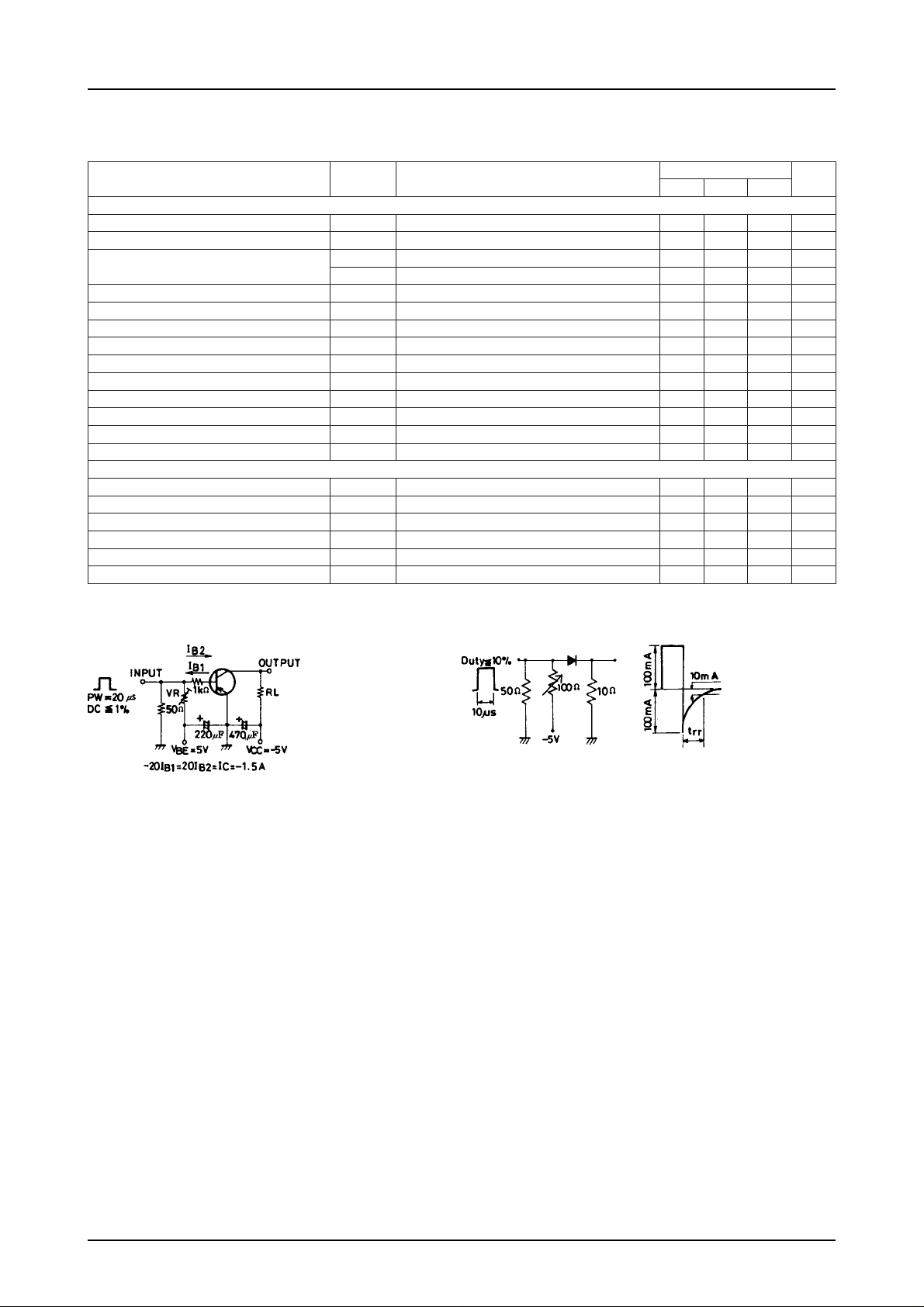
Switching Time T est Circuit
(TR) (SBD)
No.3961-2/4
 Loading...