

SANYO FH203 Datasheet

Any and all SANYO products described or contained herein do not have specifications that can handle
applications that require extremely high levels of reliability, such as life-support systems, aircraft’s
control systems, or other applications whose failure can be reasonably expected to result in serious
physical and/or material damage. Consult with your SANYO representative nearest you before using
any SANYO products described or contained herein in such applications.
SANYO assumes no responsibility for equipment failures that result from using products at values that
exceed, even momentarily, rated values (such as maximum ratings, operating condition ranges,or other
parameters) listed in products specifications of any and all SANYO products described or contained
herein.
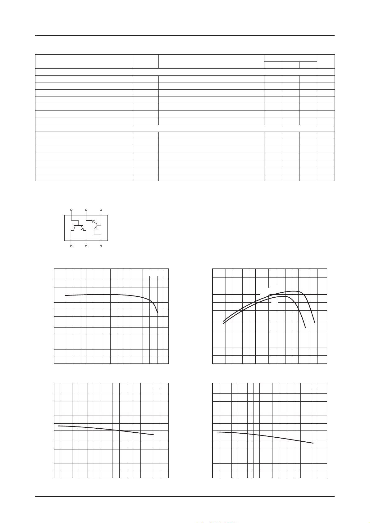
NPN Epitaxial Planar Silicon Composite Transistor
VCO OSC Circuit Applications
Ordering number:ENN6179
FH203
SANYO Electric Co.,Ltd. Semiconductor Company
TOKYO OFFICE Tokyo Bldg., 1-10, 1 Chome, Ueno, Taito-ku, TOKYO, 110-8534 JAPAN
Features
· Composite type with a buffer transistor (2SC5245)
and a oscillator transistors (2SC5415) contained in
the currently provided MCP package as a VCO
oscillator, improving the mounting efficiency greatly.
· The FH203 is formed with two chips, being equivalent to the 2SC5245 and 2SC5415, placed in one
package.
· Optimal for use in UHF band oscillator circuit.
Specifications
Absolute Maximum Ratings at Ta = 25˚C
retemaraPlobmySsnoitidnoCsgnitaRtinU
]5425CS2[1rT
egatloVesaB-ot-rotcelloCV
egatloVrettimE-ot-rotcelloCV
egatloVesaB-ot-rettimEV
tnerruCrotcelloCI
noitapissiDrotcelloCP
]5145CS2[2rT
egatloVesaB-ot-rotcelloCV
egatloVrettimE-ot-rotcelloCV
egatloVesaB-ot-rettimEV
tnerruCrotcelloCI
noitapissiDrotcelloCP
]snoitacificepsnommoC[
noitapissiDlatoTP
erutarepmeTnoitcnuJjT 051
erutarepmeTegarotSgtsT 051+ot55–
OBC
OEC
OBE
C
C
OBC
OEC
OBE
C
C
T
Package Dimensions
unit:mm
2160
[FH203]
0.25
6
12
0.65
2.0
54
3
0.2
0.4250.425
1.25
0.9
2.1
0.15
0 to 0.1
0.2
1 : Collector1
2 : Emitter1
3 : Collector2
4 : Base2
5 : Emitter2
6 : Base1
SANYO : MCP6
02V
01V
5.1V
03Am
051Wm
02V
01V
2V
001Am
051Wm
002Wm
˚C
˚C
N0199TS (KOTO) TA-1709 No.6179–1/9
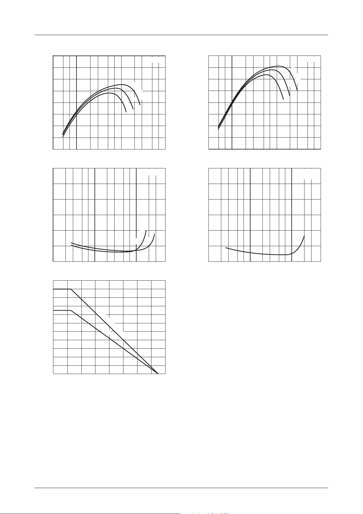
Electrical Characteristics at Ta = 25˚C
retemaraPlobmySsnoitidnoC
]5425CS2[1rT
tnerruCffotuCrotcelloCI
tnerruCffotuCrettimEI
niaGtnerruCCD
tcudorPhtdiwdnaB-niaGf
ecnaticapaCtuptuO
niaGrefsnarTdrawroF
erugiFesioN
]5145CS2[2rT
tnerruCffotuCrotcelloCI
tnerruCffotuCrettimEI
niaGtnerruCCD
tcudorPhtdiwdnaB-niaGf
ecnaticapaCtuptuO
niaGrefsnarTdrawroF
erugiFesioN
Marking : 203
Electrical Connection
E2
B2B1
OBC
OBE
h
EF
T
boC
2
|e12S|
FNVECI,V5=
OBC
OBE
h
EF
T
boC
2
|e12S|
FNVECI,V5=
V
BC
V
BE
V
EC
V
EC
V
BC
V
EC
V
BC
V
BE
V
EC
V
EC
V
BC
V
EC
FH203
nimpytxam
I,V01=
0=0.1Aµ
E
I,V1=
0=01Aµ
C
I,V5=
Am01=
C
I,V5=
Am01=
C
zHM1=f,V01=
I,V5=
C
C
I,V01=
0=0.1Aµ
E
I,V1=
0=01Aµ
C
I,V5=
Am03=
C
I,V5=
Am03=
C
zHM1=f,V01=
I,V5=
C
C
zHG5.1=f,Am01=
zHG5.1=f,Am5=4.10.3Bd
zHG1=f,Am03=
zHG1=f,Am7=1.10.2Bd
09002
811zHG
801Bd
09002
65.7zHG
0121Bd
sgnitaR
54.07.0Fp
9.04.1Fp
tinU
Tr1
Tr2
C1 E1 C2
h
-- I
5
3
2
FE
100
7
5
3
2
DC Current Gain, h
10
7
5
23 57
0.1
5
3
2
FE
1.0
Cob -- V
C
23 571023 57
CB
[Tr1]
VCE=5V
IT00478
[Tr1]
f=1MHz
100
– GHz
T
Gain-Bandwidth Product, f
1.0
3
2
10
7
5
3
2
7
5
23 5 5 5772233
0.1
5
3
2
Collector Current, IC–mACollector Current, IC–mA
f
-- I
T
C
=5V
CE
V
1V
1.0 10
Cre -- V
CB
[Tr1]
IT00479
[Tr1]
f=1MHz
1.0
7
5
3
2
0.1
Output Capacitance, Cob – pF
7
5
7
23 57
0.1
Collector-to-Base Voltage, VCB-- V
1.0
23 2 3557
10
IT00480
1.0
7
5
3
2
0.1
7
Reverse Transfer Capacitance, Cre – pF
5
7
0.1
23 57
1.0
23 23557
Collector-to-Base Voltage, VCB-- V
10
IT00481
No.6179–2/9
FH203
16
14
–dB
12
2
10
Forward Transfer Gain, S21e
12
10
8
6
4
2
0
357
8
6
S21e
23 57 7
1.0
Collector Current, IC–mA
2
NF -- I
-- I
C
2V
1V
10 100
C
f=1.5GHz
V
CE
=5V
23 5
IT00482
f=1.5GHz
[Tr1]
[Tr1]
16
14
–dB
12
2
10
Forward Transfer Gain, S21e
12
10
8
6
4
2
0
357
8
6
S21e
2
-- I
C
1V
23 57 7
1.0
Collector Current, IC–mA
NF -- I
10 100
C
f=1GHz
V
CE
=5V
2V
23 5
VCE=2V
f=1GHz
[Tr1]
IT00483
[Tr1]
4
Noise Figure, NF – dB
2
0
23 57 2 2353
0.1
220
200
180
– mW
160
150
C
140
120
100
80
60
40
Collector Dissipation, P
20
0
0 16014012010080604020
Collector Current, IC–mA
Ambient Temperature, Ta – °C
1.0 10
P
C
57
-- Ta
Total dissipation
1 unit
V
=1V
CE
5V
IT00484
[Tr1]
IT00486
4
Noise Figure, NF – dB
2
0
23 57 2 2353
0.1
1.0 10
Collector Current, IC–mA
57
IT00485
No.6179–3/9
 Loading...