

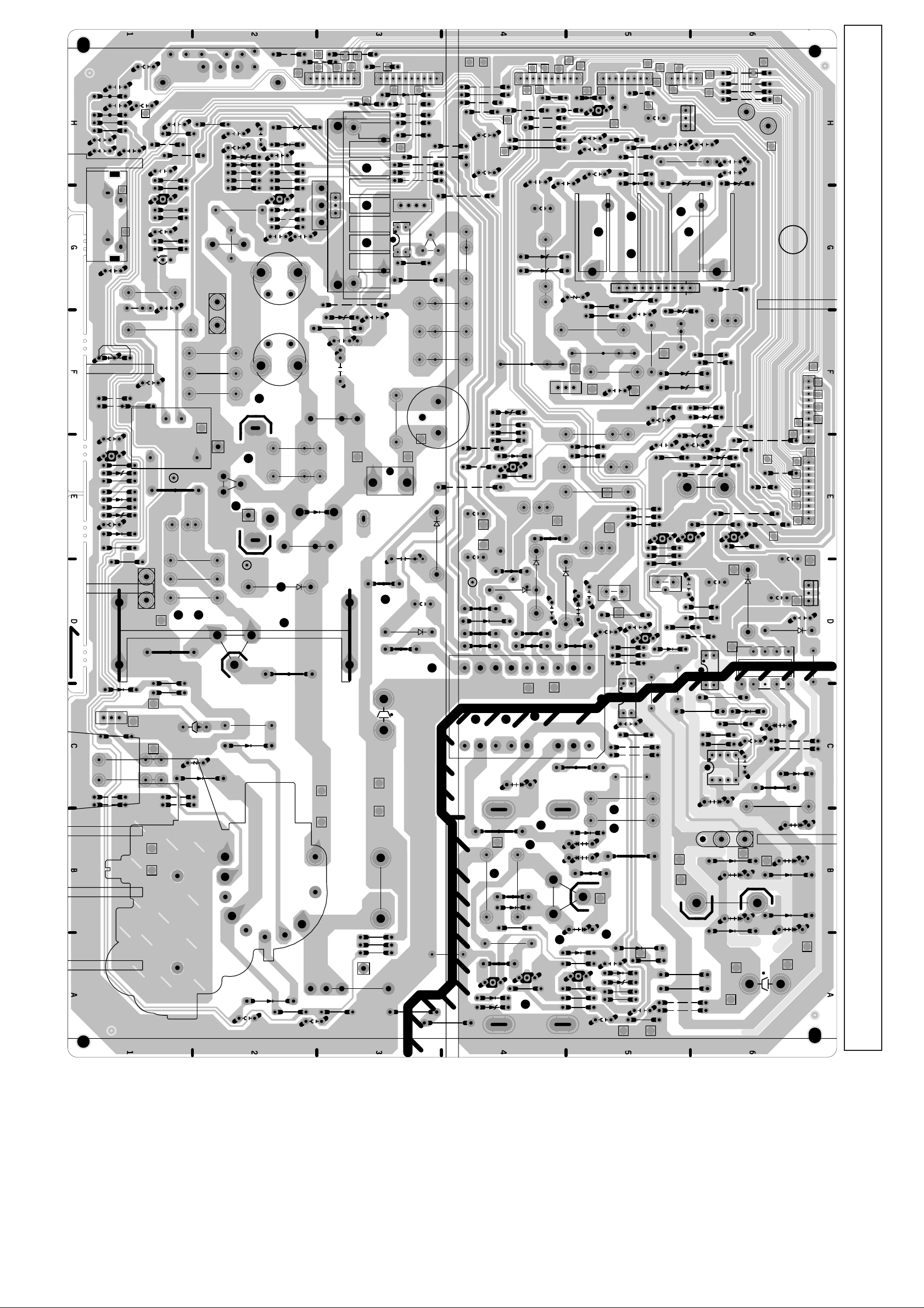
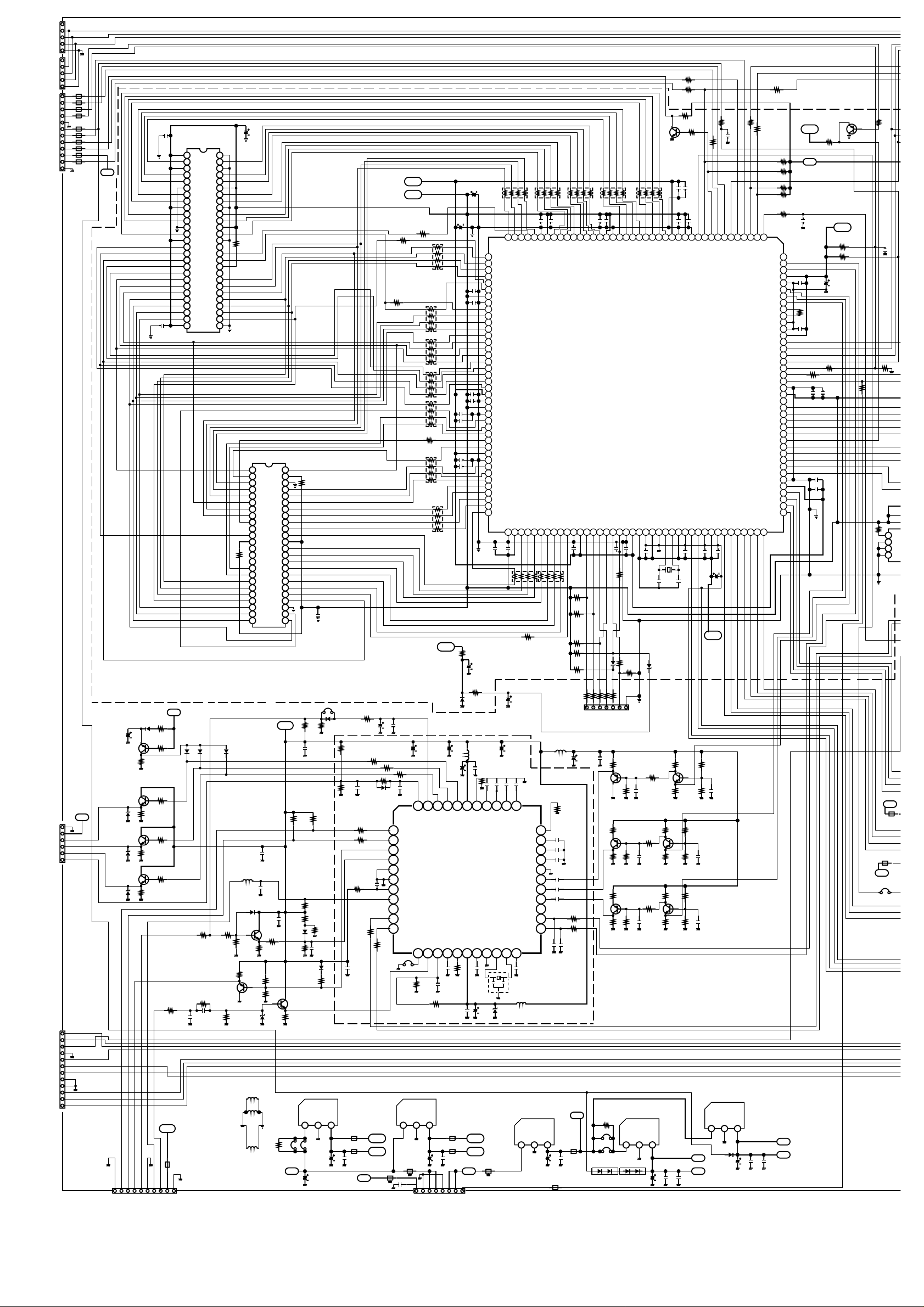
Page 1
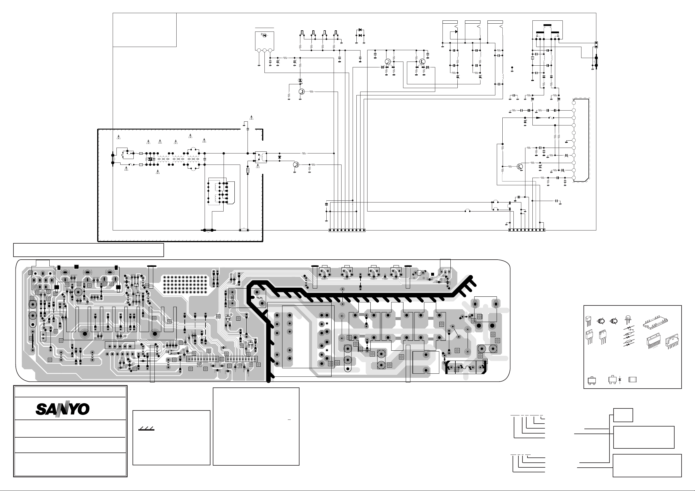
Part No. SKP20398 C6BLL (SHEET 1-5)
COLOUR TELEVISION
WW
WWBBBB6666----AAAA
SERVICE REF.NO.
MODEL NUMBER
CHASSIS SERIES
CE32FWH2F-C-00
CE32FWH2F-C
The service Precaution:
The area enclosed by this line
( ) is directly connected
with AC mains voltage. When
servicing the area, connect an
isolating transformer between
TV receiver and AC line to eliminate hazard of electric shock.
Product safety notice:
Product safety should be considered
when a component replacement is
made in any area of a receiver.
Components indicated by a mark /!\ in
this circuit diagram show components
whose values have special significance
to product safety. It is particularly recommended that only parts specified on
the part service manual be used for
components replacement pointed out
by the mark.
Circuit diagram notes :
1. All resistance values are in ohms, K=1,000, M=1,000,000.
2. All resistance rated wattages are 1/6W unless otherwise noted.
3. Excepting electrolytic capacitors, all capacitance values of less
than 1 are expressed in µF and more than 1 are pF.
4. All capacitance rated voltages are 50V unless otherwise noted.
5. All inductance values are in µH.
6. Voltage readings taken a digital voltmeter are from point indicated chassis ground. Voltage readings taken by using a colour
bar signal are with all controls at normal position. Some voltages may vary with signal strength.
7. Waveforms were taken with colour bar and controls adjusted
for normal picture. Waveforms were taken by using a wide
band oscilloscope and a low capacity probe.
ASSY,PWB,FRONT-C6BLL
8. This circuit diagram covers a basic or
representative chassis only. There
may be some components or partial
circuit differences between the actual
chassis and the circuit diagram.
9.■ Diode 1S1555 may be replaced with
1S2473,1S2076 or DS472 unless
otherwise noted.
■ Transistor 2SC536(Q,R,S),
2SC1740(Q,R,S), 2SC945A(Q,R,P)
or 2SC1815(G,O,Y) unless otherwise noted.
■ Transistor 2SA608(E,F) may be
replaced with 2SA933(Q,R),
2SA564(QA,RA), or 2SA1015(O,Y)
unless otherwise noted.
Expression of capacitance and resistance in circuit diagram.
Capacitance (Example)
1000 C M 2000 D
Characteristic
Capacitance value (220pF)
Tolerance (±20%)
Kind(Ceramic)
Rated voltage (1,000V)
Resistance (Example)
1/2 N J 1.2
Resistance value (1.2Ω)
Tolerance (±5%)
Kind (M.carbon)
Rated wattage(1/2W)
D : Carbon
N : Metallized carbon
S : Oxide metallized
W : Wire wounding
C : Solid
T, A, U, D : Electrolytic
C, K, B : Ceramic
F : Mylar film
M, N : Polypropylene
Z : Metallized paper
J= ± 5%
K= ± 10%
M= ± 20%
FRONT BOARD
Terminal guide
C : Collector
B : Base
E : Emitter
A : Anode
K : Kathode
Chip Components
(1AA0B10E68000)
PWB,FRONT-C6BLL
(1AA4B10E3220A)
CELL: 1AA0B10E68000
SW601
L601
S10B6340N
Z20103XXA:
K6A
B4Z21B0090N
X
SW601H1
F601
4A250V
TCSL
<4A >
F601A
J20B00100:
J20B00100:
J3EZ0333-:
J3EZ0333-:
J20B0170J
J20B0170J
2400010
SW601H2
L602
Z20103XXA:
B4Z21B0090N
F601B
2400010
R603
1/2DJ
220K
K6AP1
J30B0250N:
J30B1380N
K6AP2
J30B0250N:
J30B1380N
1
2
VA601
F35B1160N
ENC471
D14A
C601
250GM0.1XBC:
250HM0.1XD:
250MK0.1VA:
275GM0.1VDA
POS+ POS- VOL-VOL+
SW1951
R1901
1/16GJ
100C
D601
AA
R1953
1/16GF
1.5KC
C1903
X
Q1911
AH
S10B
1170N
Q601
AH
R1954
1/16GF
820C
R1950
390
R605
J
R/C PRE AMP.
A1901
U20B20900
321
C1901
6.3EM
470CD
C1902
KZ0.01
GQF
R1951
1/16GJ
470C
C604
250KK470XH:
400KK470XP
L605
F35B1160N
C603
L604
F35B1160N
L604H4
2400030
L604H3
2400030
L604H2
2400030
L604H1
2400030
JP601
X
L605H4
2400030
L605H3
2400030
L605H2
2400030
L605H1
2400030
JP602
X
K6AC
X
K6ACP2
J30B0250N:
J30B1380N
250GM0.1XBC:
250HM0.1XD:
250MK0.1VA:
275GM0.1VDA
L606
L26B3610N
L606H6
L606H7
2400030
2400030
L606H4
2400030
L606H3
2400030
L606H1
L606H12
2400030
12
K6ACP1
J30B0250N:
J30B1380N
RL601H2
2400030
RL601H1
2400030
PS601H1
RL601
2400030
S20B0460N:
S20B0480N
PS601
DHXAAEV0065
PS601H2
L607
X
L607H12
X
12
L607H7
X
7
L607H6
X
6
L607H4
X
4
L607H3
X
3
L607H1
X
1
2400030
J30B0250N:
J30B1380N
2400030
KEP2
KEP1
J30B0250N:
J30B1380N
1
2
KE
X
L603
L603H4
2400030
X
L603H3
2400030
L603H2
2400030
L603H1
2400030
S10B
1170N
D1951
DLXRB
0001653C
R1952
1/16GJ47KC
K11M
J11EH100N
R1955
1/16GF
5.6KC
R602
1/16GJ
56KC
SW1953SW1952
S10B
1170N
R601
1/16GJ
3.3KC
C1133
CJ100CGQ
R1956
1/16GF
2.7KC
SW1954
S10B
1170N
C1953
25KZ0.1
GQF
C1954
X
5VRC
LED
RELAY
RC_IN
KEY_SW
GND
R-FRONT
L-FRONT
TO POW&DEF
D1101
AA
D1102
AA
110
V-FRONT
C1132
KZ0.01
GQF
Q1131
AH
C1131
16EM
10CD
R1133 R1132
1/16GJ
5.6KC
R1131
1/16GJ
100KC
1/16GJ
150KC
JS1131
X
R1136
1/16GJ
100KC
JS1136
X
R1137 R1138
1/16GJ
150KC
1/16GJ
5.6KC
K1101
J31B01000
C1137
KZ0.01
GQF
Q1136
AH
C1136
16EM
10CD
C1101
X
C1102
CJ100
CGQ
R1102
1/16GJ
100KC
L1101
L2B9
100KN
R1101
1/16GJ
2.2KC
C1108
16EM
10CD
C1106
CJ100
CGQ
R1107
1/16GJ
100KC
J1131
100
L1106
L2B9
100KN
R1106
1/16GJ
2.2KC
C1107
CJ100
CGQ
C1109
16EM
10CD
J1105
J1106
VRL
K1121
J12B04901;
J12B05400
C1124
KZ0.01
C1110
X
R022
1/16GJ
47KC
R018
1/16GJ
10KC
C3523
KK
220GQ
K11E
C030
X
R009
4.7
J1104
KZ0.01
GQF
L1122
L2C1120JN
C008
25KZ0.1
GQF
C021
35EM
1000CD
Q001
AH
GQF
L1123
Z21B
0040N
C1125
X
R016
DJ680
C007
25KZ0.1
GQF
R003
1/16GJ
820C
R004
1/16GJ
10KC
R013
1/16GJ
2.7KC
C1126
16PM10K
R1122
1/2DJ
390
C011
25EM
2200CD
R010
4.7
C003
16KK0.47
(BA:GMB)
R001
1/16GJ
820C
R1111
X
J30B0250N;
J30B1380N
L1111
J
C1111
X
R015
1/16GJ
220C
X
X
9V
BBE SW
10
GND_AUDIO
L-IN
R-IN
MUTE
27V
C1121
KZ0.01
GQF
L1121
L2C1120JN
C1122
X
C1123
16PM10K
R1121
1/2DJ390
R014
DJ680
C012
25EM
2200CD
C010
C009
25KZ0.1
25KZ0.1
GQF
GQF
F001
J
R008
R006
2.2K
2.2K
C004
C006
KK0.012
25EM
GQ
33CD
R007
47
C005
R005
25EM
47
C015
25EM
47CD
33CD
C001
16KK0.47
(BA:GMB) C002
R002 IC001
1/16GJ
10KC
C3524
KK
220GQ
K11N
J11EH100N
1
KK0.012
GQ
11
10
9
8
7
6
5
4
3
2
1
K11RP2
J30B0250N
:J30B1380N
K11RP1
J30B0250N
:J30B1380N
TDA7263M
IC001H:
1AA2HEA
0062--
K11L
J10EA
020N
K11R
X
2
1
2
1
TO POW&DEF
K1121
C1124
C1121
X
K11RP2
2
L1122
L1121
K11R
X
K11RP1
1
L1123
K11L
J1122
C1126
2
R1122
1
K1101
R1111
C1110
K11E
C1111
X
C030
C1123
R1107
L1111
C1107
J1121
C1122
R1121
C1125
J001
C011
R016
R014
B10E3220A
L1106
R1106
C012
CH+CH-VOL+VOL-
R1954
L605H4L605H3
L605
JP602
KEP1
KE
21
KEP2
SW1951SW1952
C1954
R1953
L604
L604H1L605H2
X
X
L604H4L604H3
D1951
R1951
L603H3 L603H4
L603
L603H1 L603H2L604H2
PS601H2
PS601
PS601H1
A1901
C1902
R1901
C1901
SW601
L601
VA601
X
R603
L602
F601B
C601
F601
T4AH250V
T2AL250V
X
SW601H1SW601H2
K6AP1K6AP2
X
X
21
K6A
F601A
B
B
C
E
E
C
B
E
C
K
K
E
C
B
C
E
B
Transistor
C
B
Diode
K
A
E
A
K
A
A
Resistor
123
1
12 x 103= 12kΩ
N/2
N/2 + 1
N
10
9
3
2
1
7
6
5
4
3
2
1
R1133
JS1131
C1101
C1106
R1101
R1102
C1102
L1101
R006
R010
C010
C009
IC001 111
R1132
C1132
C1108
C1109
R008
C007
C008
210
C003
C004
R004
C015
C1131
R1131
Q1131
Q1136
R1136
R1137
R009
R003
JS1136
J002
R005
C1136
R1138
C1137
J1131
J1103
J1115
J005
J006
R002
C002
C001
R001
C006
R018
Q001
C021
F001
C005
R013
R007
J1110
C3523
C3524
R015
R022
1
D1102
D1101
J1952
D601
Q601
R601
R602
J1102
J1109
10 10
1
J1104 J1106J1105
C1133
J1108
J1951
RL601
J601
R1950
RL601H2
RL601H1
L606H7
R605
12 7
L606H12
L606
J602
Q1911
R1952
K11MK11N
C1953
J1107
C1903
L607H7
L607H12
L606H6
L606H4
L606H3
L606H1
SW1954
L607H4
L607H3
L607H6
R1956
61
R1955
SW1953
X
C604
C603
L605H1
X
L607
L607H1
K6AC
XX
K6ACP1 K6ACP2
12
J1953
JP601
DANGER LIVE MAINS
Page 2
POWER & DEFLECTION BOARD
L1091
L1092
C1096
C1095
WB6A
R1092
R1091
K1004
C491
E
VIDEO
3
J448
J449
C487
Q487
HEATER
K4C
J444
J443
C1093
C1094
C1098
J447
D487
R488
R487
D433
R436
D434
D435
R435
R489
D431
R446
R437
R434
C1097
L
R
XX
C432
R447
Q411H6
Q411H7
1
C1091
C1092
J476
C403
R419
R400
E
R402
R403
C401
R404
R405
E
Q402
R406
C404
C406
R408
C402
J446
T401
JWB
TP-4A1 TP-4A2
12
XX
TP-4A
L411
R433
R432
J442
J441
C400
R401
L401
J480
C405
Q401
R409A
R409
R410
C431
C438
D441
L451AH1
35V
R461
TP-4C2TP-4C1
C464
C465
C466
E
L451A
XX
X
D461H3
D461H1
Q411H1
T402H9T402H10
T402H7
5V
L451
C454
TP-4C
21
D461P
D461
Q411
C460
D455
D454
R457
R456
R459
TP-4B
JWC
Q411H2
6V
R456A
D461H2
X
R431
HEATER
ABL
C436
L451AH2
Q411H3
B
D432
C459
E
L462H2
L461H2
D412
T402
D436
J478
J479
8
D458
D457
C458
R460
R458
R471
R453
Q451
D453
J477
R454
C455C456
L462H1
L462
L461
L461H1
C462
C461
D411H3
D411H1 D411H2
C412
L412
T402H3
VIDEO
T402H4
R443
KD
GND
GND
MUTE
A-OUT-R
A-OUT-L
BBE-CNTL
MONOUT-R
MONOUT-L
Q452H4
Q452
Q452H1
EB
Q452H2
C
Q453
Q452H3
Q453A
Q452H5
J461
D421
C416
AFC
C415
C411
C411H3
C412H1C412H2
C418H3
C418H2
R442
R438
R439
R440
C411H1
C411H2
D411
C412H3
T402H1
+B
C418H4
C443
1
Q411H4Q411H5
C418
J475
K4AH1
R441H1R441H2
X
10
D654
R411
C642
J474
Q452H7
Q452H6
R441
C418P
GND
8V
K4A
L646
C418H1
C417
R425
AFC
H
D1631
J473
J469
J467
J466
IC421
21
43
K4AH2
C632
D631
L631
C642H2C642H1
J464
J471
J472
K4D
KC
R422
J436
R514
R515
PITTARI
8V-ON
C516
POW-ON
J438
J435
C515
KF
PROTECT
GND
R646
RC-IN
KEY_SW
C514
RELAY
J437
1
LED
D437
E
Q436
C512A
C512
C513
GND
VD+
VD-EWABL
J482
1
R421
J481
J483
J465
J468
41
J439
10
C1631
C1632
D
C632Z
C641
Q421
R423
C422
C423
C424
L422H2
L422
L422H1
SG
D632
J417
C421
C643
C644
J418
J419
-15V
35V
D508
D507
L503
6V
15V
D639
R636
R635
R634
D638
E
Q631
R637
C646
L644
D636
JWA
D634
L648
D633
L633
L632 L637
T611H12
T611H11
L634
L636
T611H13
R510
L645
C636
K4B
C506
31
D637
T611H17
IC501H2
R508
R503
D572
D652
R662
R655
C647
C638
C637Z
C637
T611
T611H2
T611H3
L614
D612
C619
R631
T611H5
Q613-H3
Q613-H1
Q613
L616
D611
C617Z
C617
C616Z
C616
L613
Q613-H2
C615
C615Z
D615
R627
E
Q625
R614
R611
R622
C619Z
Q611
E
R623
R629
C629
R628
R633
R613
E
T611H8
L612
R624
L615
Q612
D617
D616
6V
KB
8
GND
R512
IC501H3
R507
R509
L502
R506
C510
IC631
3
1
2
R641
C650
R642
R643
J411
D610
12
C610
J404
J403
X
C618
R625
L611
MAINS
C614
R617
R616
C613
RC5V
J434
J433
D511
8
R513
C649
34
R615
J455
C517
GND
R511
J416
J415
J414
E
Q642
GND
33V
1
5
FRONT-L
C1615
C511A
D512
46
IC501
D509
L501
R505
D505
D506
R572
C574
C662
R651
R656H2
E
R645
R1616
R644
1
3
2
IC1611
R1612
Q641
D645
C627
C628
R626
DANGER
LIVE
D614
R619
D618
D619
J402
C611
R612
J401
FRONT-R
R504
2
L501A
E
R621
R620
KG
FRONT-V
IC501H4
110
D661
C661
Q1612
C1613
J412
1
IC1613
C511
D571
J422
R1613
R1611
1
4
R1601
R571
J431
D575
J423
R656
R1615
C1611
R1604
R1605
1
8
C1601
R610H1
J454
J453
J452
J451
K4F
X
C508
C509
D504
IC501H1
J432
C505
J427
J426
D651
R656H1
E
R1614
D1603
2
3
R1603
D1601
R1602
4
IC1601
5
C1601Z
KACP1 KACP2
XX
KAC
1
D606
C606
R610
C608
D608
C609H1
C1603
C1602
C606Z
C608Z
K4E
33V
J421
Q1611
D1612
7
2
B10E31900 A
X
KN
1
J425
J424
J429
C609
C1607Z
L1601
C1612
R610H2
J428
T1601
C1607
R1607
KEY_SW
LED
C1614
D1611
10
C605
D605
D607
C607
BBE
J406
J405
27V
MUTE
L-OUT
R-OUT
GND
FR-L
FR-R
RC-IN
RELAY
5V-RC
D1602
C1605
C609H2
8V
FR-V
IC1612
C1621
15
10 10
GND
1
GND
KM
C1606
C1605Z
C605Z
C607Z
5V-RC
Page 3
Part No. SKP20398 C6BLL (SHEET 2-5)
TO
G
M
4
FRONT
POW/DEF
J10EA060N
TO
CRT
TO
AUDIO_AMP
TO
FRONT
POW/DEF
K1GG
X
TO
K1P
TO
K1G
J10EF050N
1
FRONT_V-IN
5
1
5
L841
1
L842
L843
L844
L845
L846
L849
L847
10
L848
L841/-/L849
12
0870G
0870G
0870G
0870G
0870G
0870G
0870G
0870G
0870G
K1F
J10EF100N
9V
1
R-OUT
G-OUT
B-OUT
IK-IN
6
K1D
J10EF080N
1
A-OUT_R
A-OUT_L
MUTE
BBE_CONT.
MONITOR R-OUT
MONITOR L-OUT
8
10
12
FRONT_R-IN
FRONT_L-IN
LED
KEY_SW
RC_IN
RELAY
PROTECT
POWER_ON
8V_ON
<P-TARI>
<RAST.CONT>
C842
25KZ
0.1
GQF
L850
HVCC
8V
L26B
L26B
L26B
L26B
L26B
L26B
L26B
L26B
L26B
L850
1/16
GZ0C
C843
25KZ
0.1GQF
6V
R249
1/16GJ
D241
390C
1SS355
C222
<INDP. HP_R>
<INDP. HP_L>
<HP_CONT.>
10EM
1000CD
Q233
2SA1037AKR:
2SA1179NM6P:
TXXKBB001P:
TXXKBB002P:
TXXKBB003P
Q235
2SC2412KR:
2SC2812NL6P:
TXXKBB004P:
TXXKBB005P:
TXXKBB006P
D253
UDZS12BG
Q236
2SC2412KR:
2SC2812NL6P:
TXXKBB004P:
TXXKBB005P:
TXXKBB006P
D254
UDZS12BG
Q237
2SC2412KR:
2SC2812NL6P:
TXXKBB004P:
TXXKBB005P:
TXXKBB006P
D255
UDZS12BG
R262
1/16GJ
10KC
R263
1/16GJ
470C
R270
1/16GJ
470C
R271
1/16GJ
470C
R261
1/16GJ
1KC
1/16GJ
R264
56C
R266
1/16GJ
56C
1/16GJ2.2KC
R274
1/16GJ
56C
Q261
2SC2412KR:
2SC2812NL6P:
TXXKBB004P:
TXXKBB005P:
TXXKBB006P
R283
9V
GND
K1C
J10EF100N
V-DRIVE +
V-DRIVE -
E/W
ABL
TO
H-GND
H-OUT
AFC
9V
110
POE/DEF
IC803
QXXAVC092M
<128MB-SDRAM>
1
VCC1 VSS3
2
DQ0
3
VCCQ1
4
DQ1
5
DQ2
6
VSSQ1
7
DQ3
8
DQ4
9
VCCQ2
10
DQ5
11
DQ6
12
VSSQ2
13
DQ7
14
VCC2
15
LDQM
16
WE
17
CAS
18
RAS
19
CS
20
BA0
21
BA1
22
A10
23
A0
24
A1
25
A2
26
A3
27 28
VCC3
D238D237 D239
1SS3551SS355 1SS355
1/16GJ
220C
1/16GJ10KC
C273
KK270
GQ
XL1671
1/16GZ0C
GND
DQ15
VSSQ5
DQ14
DQ13
VCCQ5
DQ12
DQ11
VSSQ4
DQ10
DQ9
VCCQ3
DQ8
VSS2
NC2
UDQM
CLK
CKE
NC1
A11
A9
A8
A7
A6
A5
A4
VSS1
R844
1/16
GJ
100C
R260
Q262
2SA1037AKR:
2SA1179NM6P:
TXXKBB001P:
TXXKBB002P:
TXXKBB003P
R272
C272
500KK
100A
54
53
52
51
50
49
48
47
46
45
44
43
42
41
40
39
38
37
36
35
34
33
32
31
30
29
R259
1/16GJ
120KC
R258
1/16GJ
100KC
10EM22CD
L2C41R0KJ
D262
1SS355
R275
1/16GJ
33KC
C841
R831
1/16GJ
10KC
10
11
12
13
14
15
16
17
18
19
20
21
22
23
L233
C259
CJ180
CGQ
R257
1/16GJ
R276
1/16GJ
2.2KC
Q262
1/16GJ
5.6KC
D264
UDZS
6.8BG
L891
L893
L1670
1/16GZ0C
1
A15 A16
A14
2
A13
3
A12
4
A11
5
A10
6
A9
7
A8
8
9
A19
NC
W
RP
NC
NC
RB
A18
A17
A7
A6
A5
A4
A3
A2
A1 A0
R279
X
X
C370
KZ0.01
GQF
C253
KZ0.01
GQF
Q261
1/16GJ680C
47C
R1671
2SJ5.6
48
BYTE
47
VSS
46
DQ15A-1
45
DQ7
44
DQ14
43
DQ6
42
DQ13
41
DQ5
40
DQ12
39
DQ4
38
VCC
37
DQ11
36
DQ3
35
DQ10
34
DQ2
33
DQ9
32
DQ1
31
DQ8
30
DQ0
29
G
28
VSS
27
E
26
2524
M29W160DT7NM
<M29W160DT
16M FLASH>
R268
X
HVCC
9V
C267
KZ0.01
GQF
R345 R343
1/16GJ
6.8KC
D261
X
R256
R255
X
R278
1/16GJ
6.8KC
Q263
2SC2412KR:
2SC2812NL6P:
TXXKBB004P:
TXXKBB005P:
TXXKBB006P
R273
1/16GJ
1.8KC
JS1673
RC5V
R843
1/16GJ
100C
C844
25KZ
0.1
GQF
IC802
R269
X
1/16GJ
6.8KC
R251
1/16GJ
1KC
R253
X
R254
X
X
C251
D263
X
R277
X
123
JS1671
X
C1673
16EM
10CD
C1677
10EM100CD
JS258
1/16GZ0C
D258
X
R235
1/16GJ
33KC
R245
1/16GJ
22KC
R232
R231
R265
1/16GJ
10KC
1/16GJ
220C
1/16GJ
220C
C252
KZ0.01
GQF
IC1672
TA48018S:
BA18BC0T
<1.8V>
L1673
L26B2770G
L1674
L26B2770G
C1674
KZ0.01
GQF
R267
1/16GJ
220C
C271
16EM
10CD
R246
1/16GJ
100C
R250
1/16GJ
10KC
C263
KK470
GQ
1/16GJ100C
1/16GJ100C
C264
16KK
0.1GQ
R236
R237
RC1V8A
RC1V8
33V
C3400TM
KZ0.01F
RB806,8-10
R1A43304G;
R1A43304G;
R1A43304G;
R1A43304G;
R1EA3304G
R1EA3304G
R1EA3304G
R1EA3304G
R247
1/16GJ100C
D251
1SS355
XL1672
1/16GZ0C
POE/DEF
RC1V8
RC3V3
C808
10EM GQF
R800
22CD
1/16GJ
33C
R801
RB806
1/16GJ
33C
RB808
CJ390
CGQ
R802
1/16GJ
27C
RB809
RB810
25KZ
0.1
RB811
GQF
25KZ
0.1
GQF
R834
1/16GJ
33C
C812
RB812
25KZ
0.1
GQF
C857
CJ390
CGQ
RB813
RB811-3
R1A43304G;
R1A43304G;
R1A43304G;
R1EA3304G
R1EA3304G
R1EA3304G
RC3V3
D803
1SS355
C270
KK
1000GQ
C266
10EM
470CD
R248
1/16GJ100C
C261
CJ47
CGQ
C265
X
C257
10EM
47CD
44 43 42 41 40 39 38 37 36 35 34
INIKIN
ABL
V-DRIVE V-DRIVE +
E-W OUT
EHT IN
FLASH IN
GND
DIGITAL SUPPLY
DECOUPLING
HORIZONTAL
OUT
SANDCASTLE
PULSE OUT
IIC
SCL
IIC
SDA
H-PULSE IN
H-FREQ.
SELECT OF
C274
R286
KZ
1/16GJ
0.01
33KC
GQF
R285
1/16GJ33KC
123
C1671
16EM
10CD
XL1673
1/16GZ0C
BLUE OUT
GREEN OUT
QXXAVB544P:
QXXAVC186P
<TDA9330H-N2C>
CAPACITOR
VERTICAL SAWTOOTH
COMPENSATION
DINAMIC PHASE
C231 C234
GJ0.1T
:HJ0.1G
R238
1/16GJ
39KC
C233
KZ0.01
GQF
IC1671
BA033T
;TA48033S
<3.3V>
L1671
L26B2770G
L1672
L26B2770G
C1672
KZ0.01
GQF
10
11
JS211
X
1
2
3
4
5
6
7
8
9
1
33V_IN
GND
RC5V_IN
TO
RB805 RB804 RB803 RB802 RB801
C807
10EM22CD
4039383736353433323130292827262524232221201918171615141312111098765432
41
ADDR_8
42
ADDR_7
43
ADDR_6
ADDR_5
44
45
X
1/16GJ
270C
RB814/5
R1A43304G;
R1A43304G;
R1EA3304G
R1EA3304G
R841
1/16GJ
1KC
C829
10EM47CD
R842
L232
L2C4330KJ
C256
KZ0.01
GQF
1/16GZ
0C
ADDR_4
46
CKOUT_SDRAM
VDD33_IO
47
48
VSS_IO
49
CKIN_SDRAM
ADDR_3
50
ADDR_2
51
ADDR_1
52
53
ADDR_0
54
ADDR_10
55
ADDR_16
56
ADDR_15
57
NOT_CS_SDRAM
58
NOT_RAS
59
NOT_CAS
60
RD_NOTWR
61
NOT_BE0
62
VDD18_CORE
63
VSS
64
VDD33_IO
65
VSS_IO
66
NOT_CS_FLASH
67
ADDR_17
68
ADDR_18
69
ADDR_19
70
ADDR_14
71
VDD18_CORE
72
VSS
73
FLASH_D15
74
FLASH_D7
75
FLASH_D14
76
FLASH_D6
77
FLASH_D13
FLASH_D5
78
FLASH
79
_D12
80
FLASH
_D4
C858
CJ390
CGQ
C813
25KZ
0.1
GQF
RB814
C247
R243
25KZ0.1
GQF
C269
X
C854
C809
25KZ
0.1
GQF
C855
C810
C811
C856
CJ390
CGQ
C249
VCC
B-2 IN
R-2 IN
G-2 IN
BLK-2 IN
RED OUT
IC202
FIXED BEAM
CURRENT
SWITCH-OFF
Y-SIGNAL IN
U-SIGNAL IN
V-SIGNAL IN
DAC OUT
X-TAL OUT
X-TAL IN
GND
BANDGAP DECOUPLING
VCC
REFERENCE CURRENT IN
GJ0.1T
:HJ0.1G
RC3V3A
RC3V3
6V
K1B
8
J10EF080N
6V_IN
H-PROTECT
1/16GZ0C
XL1674
C232
10EM
47CD
L2C4330KJ
D256
UDZS12BG
C852
ADDR_9
ADDR_11
C806
25KZ
0.1
ADDR_12
NOT_EE1
VSS_IO
ADDR_13
C853
CJ390
CGQ
VDD33_IO
SDRAM_D8
SDRAM_D9
SDRAM_D12
SDRAM_D11
SDRAM_D10
CJ390
CGQ
SDRAM_D15
SDRAM_D14
SDRAM_D13
QXXAVC178M
<STV3500>
VSS_IO
VDD33_IO
FLASH_D11
FLASH_D3
FLASH_D10
FLASH_D2
FLASH_D9
FLASH_D1
FLASH_D8
FLASH_D0
VSS
VDD18_CORE
TMS
TCK
TDO
C815
25KZ
0.1
GQF
RB815
R851
1/16
GJ
10KC
R852
1/16
GJ
10KC
RESET
OUT
C244
16KK
0.047GQ
BLK
-1
IN
B-1
IN
G-1
IN
R-1
IN
HD
IN
VD
IN
BA05T
C1679
16EM
10CD
L201
L2C4100KJ
33
32
31
30
29
28
27
26
25
24
23
C238
CC10
CGQ
L1678
L26B0870G
R853
1/16GJ
10KC
R854
1/16GJ
10KC
R856
1/16GJ
10KC
J10EA070N
C201
10EM
100CD
R242
1/16GZ
0C
C225
C224
C223
C243
C242
C241
L1675
1/16GZ
KJTAG
25KZ0.1
GQF
25KZ0.1
GQF
25KZ0.1
GQF
25KZ0.1
GQF
25KZ0.1
GQF
25KZ0.1
GQF
1/16GJ
100C
C237
CJ27
CGQ
0C
C1678
KZ0.01
GQF
R241
R239
1/16GJ
100C
5V
R857
TMS
C202
25KZ0.1
GQF
R858
TCK
JS1674
D1673
DCC010
R859
TDI
R1672
2SJ5.6
XX
JS1672
X
R819
1/16GJ
33C
C830
16EM10CD
C248
PEAK
LIMITING
SUPPLY
START-UP
LOW-POWER
2221201918171615141312
C236
GJ0.1T
:HJ0.1G
X231
V11B00100
L231
IC1674
123 321
C805
VDD33_IO
TDI
25KZ0.1GQF
C814
R861
R860
TDO
R208
1/16GJ
1KC
R215
1/16GJ
1KC
25KZ
0.1
GQF
VSS_IO
SDRAM_D1
SDRAM_D0
IC801
TRST
NRESET
VSS
99989796959493929190898887868584838281
C816
R845
1/16GJ100C
C816
25KZ
0.1
GQF
D851
1SS355
R862
1/16GJ
100C
R855
1/16GJ
10KC
71
TRST
NRESET
NRESET
L202 L203
R201
1/16GJ
1KC
Q201
R202
1/16GJ
C205
1.5KC
X
R207
1/16GJ
390C
Q203
R209
1/16GJ
3.9KC
R214
1/16GJ
470C
Q205
R216
1/16GJ
15KC
IC1676
TA48018S:
BA18BC0T
D1674
DCC010
SDRAM_D5
SDRAM_D4
SDRAM_D3
SDRAM_D2
VDD18_CORE
VDD18_IO
GND_IO
VDD18_PLL3
103102101100
25KZ
0.1
GQF
C820
CD6
CGQ
D852
1SS355
R857-R862
R221
1/16GZ
0C
R210
1/16GJ
180C
R222
1/16GZ
0C
C209
X
R217
1/16GJ
180C
R223
1/16GZ
0C
C212
X
C1681
16EM
10CD
RB801-5
R1A43304G;
R1A43304G;
R1A43304G;
R1A43304G;
R1A43304G;
R1EA3304G
R1EA3304G
R1EA3304G
R1EA3304G
R1EA3304G
SDRAM_D6
GND_PLL3
1/16GJ
100C
<1.8V>
KZ0.01
C1682
GQF
1/16GZ0C
R826
JP801
X
R881
1/16GJ
1KC
Q814
R880
1/16GZ
0C
R830
1/16GJ
100C
C802
C851
25KZ
CJ390
0.1
CGQ
GQF
FRONT-SC3
PLL_LOCK
C850
C801
CJ390
25KZ
CGQ
0.1
GQF
P-TARI
RASTER CONT. /
VSS_IO
VDD33_IO
VSS
SDRAM_D7
VDD18_CORE
PORTD6/INT0
PORTA3/PWMCAP3/PWM3
PORTA2/PWMCAP2/INT3/EXT/PWM2
PORTD7/INT1/16XUART CLOCK
PORTA1/PWMCAP1/INT2/PWM1
PORTA0/PWMCAP0/PWM0 (NRESET OUT)
XTALIN
XTALOUT
VCC18_PLL1
GND_PLL1
CLKXTM
CLKXTP
VSS_PLL
VDD18_PLL
C823
C821
CD6
CGQ
25KZ
0.1
GQF
C818
10EM
22CD
C859
X
X801
V10B4810N
<27MHZ>
C822C819
CJ390
CGQ
RC1V8A
R203
1/16GJ
R205
390C
1/16GJ
1KC
Q204
R211
1/16GJ
68C
Q206
R218
1/16GJ
68C
Q202
R204
1/16GJ
68C
1/16GJ
220C
1/16GJ
220C
R213
R220
R206
1/16GJ
220C
R212
1/16GJ
1KC
R219
1/16GJ
1KC
C211
25KZ0.1
GQF
C214
25KZ0.1
GQF
C208
25KZ0.1
GQF
A-OUT_L
<1V8A>
1V8
1V8
C1683
KZ
0.01GQF
R829
1/16GJ
1KC
KK
C839
4700
GQ
R827
1/16GJ
100C
POWER_ON
LED
SC3_8P
RELAY
PORTD3/TIMER IN 3/OUT 2
AV_SW2
AV_SW1
8V_ON
SOUND_INT
PORTC5/SCL_2
PORTC6/SDA_3
PORTC4/SDA_2
VCC33_DAC
PORTD1/TIMER IN 1
PORTD0/TIMER IN 0
GND_DAC
PORTD2/TIMER IN 2/OUT 3
GND_REXT
SHIELD_ADCDAC
GND_ADC
VCC33_ADC
PORTD5/GFX_ACTIVE
PORTB0/AD_0
PORTB1/AD_1
PORTB2/AD_2
PORTB3/AD_3
PORTB4/AD_4/TIMER OUT0
PORTB5/AD_5/TIMER OUT1
VDD33_IO
PORTA7/RTS
PORTA6/CTS
PORTA5/RXD
PORTA4/TXD
PORTD4/IR_IN
PORTC0/SDA_0
PORTC1/SCL_0
PORTC2/SDA_1
PORTC3/SCL_1
VDD18_CORE
YCRCB7
YCRCB6
YCRCB5
YCRCB4
SHIELD_PLL
VSYNC
HSYNC
CLK_DATA
YCRCB0
YCRCB1
YCRCB2
YCRCB3
120119118117116115114113112111110109108107106105104
Q202/4/6
2SC2412KR:
2SC2412KR:
2SC2412KR:
2SC2812NL6P:
2SC2812NL6P:
2SC2812NL6P:
TXXKBB004P:
TXXKBB004P:
TXXKBB004P:
TXXKBB005P:
TXXKBB005P:
TXXKBB005P:
TXXKBB006P
TXXKBB006P
TXXKBB006P
Q201/3/5
2SA1037AKR:
2SA1037AKR:
2SA1037AKR:
2SA1179NM6P:
2SA1179NM6P:
2SA1179NM6P:
TXXKBB001P:
TXXKBB001P:
TXXKBB001P:
TXXKBB002P:
TXXKBB002P:
TXXKBB002P:
TXXKBB003P
TXXKBB003P
TXXKBB003P
A-OUT_R
IC1675
BA033T
;TA48033S
<3.3V>
321
C1676
D1675
KZ0.01
1SS355
GQF
C1675
6.3EM
3300CD
JP802
X
R828
1/16GJ
100C
R821
1/16GJ
10KC
R820
1/16GJ
100C
1
CLK
160
_DFL
H100
159
158
V100
PORTC7/SCL_3
157
156
155
Y_G
154
PR_R
153
PB_B
152
151
REXT
150
149
148
147
146
145
144
143
142
141
140
VSS_IO
139
138
137
136
135
134
133
132
131
130
129
128
127
126
VSS
125
124
123
122
121
MUTE
3V3
3V3
C1670
KK
0.01GQ
<AV SW1>
<AV SW2>
<FRONT/SCART_3 SW>
Q814
2SC2412KR:
2SC2812NL6P:
TXXKBB004P:
TXXKBB005P:
TXXKBB006P
RC3V3
RC5V
R822
1/16GJ
10KC
1/16GJ
R824
10KC
1/16GJ
R825
10KC
C838
25KZ
0.1
GQF
C835
25KZ
0.1
GQF
R813
1/16GF
10KC
C834
CJ390
CGQ
AUDIO_MUTE
SC1_8P
SC2_8P
PROTECT
R814
KEY_SW
R817
AGC
H-PROTECT
C831
CJ390
CGQ
ACK
STATUS
USB2
USB1
AV-LINK_IN
AV-LINK_OUT
RC_IN
NRESET OUT
SDA
SCL
SDA_NVM
SCL_NVM
PB_B
SCL
<3V3A>
R876
1/16GJ
10KC
10EM22CD
1/16GZ0C
1/16GZ0C
C832
25KZ
0.1
GQF
C825
CJ390
CGQ
C824
25KZ
0.1
GQF
PR_R
Y_G
SDA
2SA1179NM6P:
Q811
RC3V3A
R872
1/16GF
1KC
R823
C836
V100
Q811
2SA1037AKR:
TXXKBB001P:
TXXKBB002P:
TXXKBB003P
1/16GJ
39KC
H100
JP2002
R816
1/16GJ
100KC
C833
25KZ
0.1
GQF
X
R869
1/16GJ
39KC
R877
1/16
GJ1KC
1
2
3
4
IC80
M24C64WMN6
<64K-NVM>
3V3
L2005
L26B2770
L2006
L26B2770G
1V8
1/16GZ
0C
R815
VSS
NC
NC
NC
Page 4

SC2_8
SC1_8
SC3_8
Z801
Z802
1AA2SHF0471-1AA2SHF0472--
R874
R873
X
1/16GJ
15KC
R868
1/16GJ
10KC
AV_LINK_IN
R807
1/16GJ
100C
R808
1/16GJ
100C
R805
1/16GJ
10KC
VCC
8
WC
7
SCL
6
SDA
5
STV8206_CLOCK
L2007
RB2001
C2023
CJ390
CGQ
RB2002
C2026
CJ390
CGQ
RB2003
RB2001-3
R1A46804G;
R1A46804G;
R1A46804G;
R1EA6804G
R1EA6804G
R1EA6804G
R875
1/16GJ
15KC
AV_LINK_OUT
R809
1/16GJ
10KC
R806
1/16GJ
10KC
SOUND_INT
L2009
X
X
1/16GZ0C
C2067
CJ68
CGQ
C2022
10EM
C2021
22CD
25KZ
0.1GQF
C2024
25KZ
0.1GQF
C2025
10EM
22CD
Gronding-Connect
From
TP-F
CJ180CGQ
J10MA010N
C863
12
AV_LINK
R870
AGC
R810
1/16GJ
10KC
1/16GJ
100C
1/16GJ
100C
L2010
C2011
25KZ
0.1GQF
TO
BBE
AFT
L862
R811
R812
X
L861
X
SDA
R2005
1/16GJ
100C
R803
C827
CJ22
CGQ
C826
25KZ
0.1
GQF
SCL
1/16GJ22KC
R871
1/16GJ
100KC
RC5V
L863
X
R866
R864
X
C862
X
R867
X
1
3
J10AN070N
1/16GJ
10KC
RC3V3
L2008
1/16GZ
0C
C2007
25KZ
0.1GQF
17
VDD18
_CORE
18
VSS
19
YCRCB7
20
YCRCB6
21
YCRCB5
22
YCRCB4
23
VSS_IO
24
VDD33_IO
25
YCRCB3
26
YCRCB2
27
YCRCB1
28
YCRCB0
29
VDD18_OUT
VSS_OUT
30
31
CLK_DATA
32
PLL_LOCK
H_SYNC
33 34 35 36 37 38 39 40 41 42 43 44 45 46 47 48
R865
X
X
C861
D861
X
X
D862
X
Q861
X
R863
X
USB1
USB2
X
GND
KUSB
7
NV_SCL
NV_SDA
RC3V3
STATUS
SCL
SDA
GND
1
KCPA
1/16GJ
10KC
C828
CJ22
CGQ
MUTE
R804
R2006
1/16GJ
100C
I2CADD
VSS_IO
VDD33_IO
R818
1/16GJ
4.7KC
1/16GJ
100C
C2000
25KZ
0.1GQF
VSS
NRESET
C2006
CJ390
CGQ
VDD18_CORE
STV2310DM
FIELD
VCC33SUB
GNDSUB
NC
V3.1
VCC18SUB
V_SYNC
C143
CJ68
CGQ
T141
R120
1/16GJ
5.6KC
KK
390GQ
KK
0.01GQ
1/16GJ
12KC
R162
1/16GJ
10KC
SDA
SCL
IC2001
VCC18_CLK
GND_CLK
X2001
C141
KK0.01
GQ
C142
CC5CGQ
SL0004XV
C138
CJ560
CGQ
C121
C122
C123
16KK0.47
(BA:GMB)
R161
1/16GJ100C
R122
1/16GJ100C
R2003R2004
1/16GJ
100C
C2005
CJ390
CGQ
VSS
XTALOUT
25KZ
0.1GQF
X
C2056C2055
XX
A101
F1BEB0250
TUNER(WITH PLL & BAND SW)
GND
1110987654321
C113
X
C144
CC5
CGQ
X132
SF5315
:SF5315U
IF1
33V
R103
EM10CD
1/16
GJ
68C
JS112
1/16
GZ0C
C146
1/16GZ
0C
C104
C103
X
C145
KK
0.01
GQ
JS111
R105
1/16GJ
1KC
BT
N.C
C102
10EM
1000CD
L102
X
5V
JP102
1/16GZ0C
Z101
1AA2SHF0473-1AA2SHF0474--
Z102
X
R104
1/16GJ
5.6KC
X101
F32B
0360N
IC101
TDA9886TSV4P
1
SIF2
VIF1
2
SIF1
10
11
12 13
C2002
16KK
0.022GQ
C2061
X
C2004
25KZ
0.1GQF
VSS
TST_MODE
VDD18_CORE
CLKXTM
CLKSEL
SHIELD
C2017C2016
25KZ
0.1GQF
JP2001
1/16GZ
0C
VIF2
3
OP2
OP1
4
AFC
FMPLL
5
VP
DEEM
6
VPLL
AFD
7
AGND
DGND
8
CVBS
AUD
9
VAGC
TOP
REF
SDA
TAGC
SCL
SIOMAD
R125
1/16GJ
68KC
SCL
SDA
L2C45R6KJ
C2003
KK1000
GQ
R2001
1/16GJ
470C
C2009
CJ390
CGQ
12345678910111213141516
C
64
CVBS2_Y
63
VCC18_CVBS
GND_CVBS
62
CVBS1_Y
REFM_CVBS
61
REFP_CVBS
60
VIDEO_OUT
59
VIDEOCOMM
58
ADCIN
57
VCC33_IO
56
GND_IO
55
GND_DIG
54
VCC18_DIG
53
B_PB
52
G
R_PR
GND_RGB
51
VCC18_RGB
50
49
FB
REFP_RGB
REFM_RGB
C2018
25KZ
0.1GQF
C2015
JP2003
X
10EM
22CD
JP2004
1/16GZ
0C
FIRST BLANKING IN FOR RGB SCART
D3421
1SS355
C120
KK0.01
GQ
AU_TV-OUT
R121
SIF_OUT
VDD18_CORE
XTALIN_CLKXTP
BP
NC
L101
R107
1/16GZ
0C
Q141
2814F4P:
2814-F5
R106
1/16GJ
27C
1/16GJ
100C
L2001
MB
C109
KK
0.01
GQ
JP101
1/16GZ0C
X
R108
1/16GJ
220C
2SC
2SC
C147
X
R149
1/16GJ
56C
9V
SB6315T
X131A
X
24
23
L/L'
22
C132
21
KK0.01
GQ
20
19
18
17
16
15
14
R116
CJ12CGQ
SIF IN-1
AU_TV-OUT
C2053
CC10
CGQ
C2051
CJ180
CGQ
C2012
10EM
22CD
C2001
25KZ
0.1GQF
<CVBS_TUN>
C2027 C2029
CJ390
CGQ
1/16GJ
R2021
470C
C2036
25KZ
0.1GQF
C2030
25KZ
0.1GQF
C2038
C2037
C2037/8/9
16KK
0.022GQ
C2019
25KZ
0.1GQF
L2000
L26B2770G
<1V8A>
C3421
10EM
100CD
R3421
1/16GJ
10KC
DATA
6.3EM
100CD
X131
C129
16KK0.22
BA
C126
NRESET
C2028
25KZ
0.1GQF
16EM
10CD
C2039
1V8
CLOCK
C105
R145
1/16GJ
68KC
C148
KK0.01
GQ
R147
1/16GJ
10KC
R148
1/16GJ
10KC
JS134
X
C137
CJ560CGQ
C130
KK1500
GQ
R130
1/16GZ
0C
Q131
R123
1/16GJ
2.7KC
R131
1/16GJ
560C
C128
C2052
CJ270
CGQ
C2010
CJ390
CGQ
C2031
CJ180
CGQ
R2025
1/16GJ
470C
R2024
1/16GJ
470C
1/16GJ
10KC
Q3421
2SA1037AKR
R3422
1/16GJ
560C
ADDRESS
R101
1/16GJ
100C
R102
1/16GJ
100C
C149
KK0.01
GQ
R146
1/16GJ
22KC
JS132
X
D132
1SS356
1SS356
R150
1/16GJ
33KC
R119
X
R129
X
C131
KK0.01
GQ
R128
1/16GJ
330C
C134
KZ0.01
GQF
R132
X
16KK0.47
(BA:GMB)
X133
V10B6260N
<CVBS/Y_AV>
R2002
<C_AV>
1/16GJ
68C
L2002
L26B2770G
L2003
L26B2770G
C2013
10EM22CD
C2014
C2008
CJ390
10EM
CGQ
22CD
1/16GJ
R2022
150C
C2034
CJ82
CGQ
5R6KJ
C2032
CC10
CGQ
L2C4
L2026
5R6KJ
C2047
R2026
1/16GJ
CC10
470C
CGQ
C2046
CJ180
CGQ
L2025
C2044
CC10
CGQ
C2043
CJ180
CGQ
L2024
C2041 R2027
CC10
CGQ
C2040
CJ180
CGQ
3V35V
R3423
R3424
1/16GJ
2.2KC
Q3422
2SC2412KR
TU
D131
(4MHZ)
<1V8A>
1V8
L2021
L2C4
L2C4
5R6KJ
L2C4
5R6KJ
JS133
Q152
L2004
L26B
2770G
1413
GND
15
AGC
X
R152
1/16GJ
27KC
R118
1/16GJ
10KC
R126
1/16
GJ
10KC
C133
16EM10CD
R134
X
R135
X
Q132
X
JS130
1/16GZ
<3V3A>
3V3
R2029
1/16GJ
68C
C2048
CJ180
CGQ
R2028
1/16GJ
68C
C2045
CJ180
CGQ
1/16GJ
68C
C2042
CJ180
CGQ
TP-A
J10MA010N
C101
25EM
4.7CD
Q151
L132
X
R136
X
0C
TP-C
J10MA010N
C106
1/16
GZ0C
R127
1/16GJ
10KC
9V5V
R137
1/16GJ
100C
R138
1/16GJ
220C
1/16GJ
270C
C135
X
Q135
X
R143
X
Q131
2SC2412KR:
2SC2812NL6P:
TXXKBB004P:
TXXKBB005P:
TXXKBB006P
2SC2412KR:
2SC2412KR:
2SC2812NL6P:
2SC2812NL6P:
TXXKBB004P:
TXXKBB004P:
TXXKBB005P:
TXXKBB005P:
TXXKBB006P
TXXKBB006P
Q151/2
D121
1SS356
2SC2412KR:
2SC2812NL6P:
TXXKBB004P:
TXXKBB005P:
Q133
TXXKBB006P
Q133
1/16GJ
470C
R139
R141
X
C136
X
R144
Q136
X
Q134
2SA1037AKR:
2SA1179NM6P:
TXXKBB001P:
TXXKBB002P:
TXXKBB003P
<FRONT/SCART_3 SW>
R140
Q134
R142
X
X
3V3
X
1/16GZ
0C
1/16GZ
0C
<AV SW1>
<AV SW2>
R3467
R3462 R3461
XX
R3463
X
5V
JN06
1/16GZ
0C
JN07
X
JN16
1/16GZ
0C
JN17
X
C3405
16EM
10CD
C3483
25KZ
0.1GQF
C3409
X
JN11
X
X
JN12
X3451
R3468
V10B4810N
1/16
<27MHZ>
GJ
270KC
C3481
CJ12
CGQ
JN19
JN18
JN13
L3458
Q3452
X
C3410
X
C3484
25KZ
0.1GQF
C3485
25KZ
0.1GQF
C3411
X
SOUND_INT
R3466
1V8
JN05
C3479
25KZ
0.1GQF
C3408
1/16GZ
0C
C3486
25KZ
0.1GQF
C3482
CJ12
CGQ
1/16
GJ1KC
JP1201
1/16GZ
1/16GJ220C
1/16GJ220C
Q3451
X
L3456
L3457
X
X
41
42
43
44
45
46
VDD1
47
GND1
48
N/C
49
GNDSP
50
51
XTI
52
XTO
53
VDDP
54
GNDP
55
GND2
56
VDD2
57
CKTST
58
59
60
(I2S)
SIF IN-1
R1044
1/16GJ
4.7KC
2SC2412KR:
2SC2812NL6P:
TXXKBB004P:
D1042
1SS355
R1286
0C
X
(VSS18)
REG
(RESET)
SYSCK
MCK
R1260
1/16GJ1KC
(VDD18)
(VDD33_IO1)
(VSS33_IO1)
(VDD18)
(CLK_SEL)
(VCC18_CLK1)
(GND18_CLK1)
(GND18_CLK2)
(VCC18_CLK2)
TXXKBB005P:
TXXKBB006P
Q1043
R1046
1/16GJ
R1047
22KC
1/16GZ
0C
2SA1037AKR:
Q1044
2SA1179NM6P:
TXXKBB001P:
TXXKBB002P:
TXXKBB003P
9V
CTL_A
TV
C1218
R1230
CJ82
1/16GJ
CGQ
270C
L1203
L2C4
4R7KJ
C1205
25KZ
2SC2412KR:
2SC2812NL6P:
TXXKBB004P:
TXXKBB005P:
TXXKBB006P
R1215
Q1202
1/16GJ
100C
C1206
CJ22
CGQ
R1217
1/16GJ
470C
C1270
R1284
25KZ
1/16GJ
0.1GQF
270C
R1283
1/16GJ
75C
C1207
R1285
KZ
1/16GJ1KC
0.01GQF
C1259
FRONT SC-3
CJ100
CGQ
40 39 38 37 36 35 34 33 32 31 30 29 28 27 26 25 24 23 22 21
SDA
(VSS18)
(VSS33_IO2)
(VDD33_IO2)
(I2S)
SDO
C3454
CJ100CGQ
H
1
2
L
3
4
GND2
R
5
6
7
89
L
SC-3
X
IC1203
C1222
X
JP1202
JP1203
1/16GZ
C3474
16KZ1FA
C3473
16KZ1FA
C3403
X
C3404
X
C3406
X
SCL
ADR
(HPD)
(VSS18)
(VDD18)
(VSS18_CONV)
(VDD18_CONV)
<HP DETECT>
STV8216TP
<STV8206/07>
(BUS_EXP)
<BBE>
(I2S)
(VSS18)
(VDD18)
(I2S)
(I2S)
(I2S)
WS
BUS0
BUS1
SCK
ST/SDI
C3413
C3412
X
C3414
X
D1203
UDZS10BG 0.1GQF
C1225
16PM10
STV2310_C IN
L1205
L2C4
4R7KJ
C1269
CJ82CGQ
C1267
CJ100
CGQ
L
16
GND1
15
FRONT
14
H
VCC
13
12
L
11
SC-3
GND3
10
V
H
FRONT
1/16GZ
0C
0C
B
G
R
TO_FRONT
C3475
KK0.01
GQ
C3476
KK0.01
GQ
C3472
X
C3471
X
LSL
LSR
HPL
HPR
(LS_SUB)
<HP OUT-L>
<HP OUT-R>
IC3451
(SIF_P)
(GND_PSUB)
IRQ
(VSS18_ADC)
(VDD18_ADC)
SIF
C3453
1/16GZ
0C
X
R3451
X
R1034
1/16GJ
10KC
IC1201
CTL_B
SC1
C1211
CJ82
CGQ
R1206
1/16
GZ0C
L1201
EZ007
0XXA
D1202
UDZS
10BG
C1200
25KZ
0.1GQF
Q1261/2
R1261 R1263
1/16GJ
3.9KC
C1262
16EM
10CD
TO
C1261
25KZ
0.1GQF
JS1204
X
5V
R3446
1/16GJ
220C
C3433
CJ100
CGQ
C3477
16EM
10CD
C3478
25KZ
0.1GQF
AI3L
AI3R
(LS_C)
(LS_SL)
(LS_SR)
(VSS33_CONV)
(VDD33_CONV)
<SC2_MON. R-OUT>
<FRONT AV L-IN>
<FRONT AV R-IN>
<SC2_MON. L-OUT>
<SCART2 R-IN>
<SCART2 L-IN>
<SCART1 R-IN>
<SCART1 L-IN>
<SC1_TV R-OUT>
<SC1_TV L-OUT>
(GNDPW_IF)
(SIF_N)
(GND18_IF)
(VCC18_IF)
MONOIN
GNDIF
VDDIF
VREFIF
VTOP
C3455
25KZ
0.1GQF
C3452
25KZ
C3451
0.1GQF
16KK
0.22BA
5V
Q1041
R1043
1/16GJ
4.7KC
D1041
1SS355
Q1042
CTL_C
R1201
1/16
GJ
270C
X
C1264
C1271
X
L1206
SC_2R
SC_1R
C3469
(SC3_R-OUT)
(SC3_L-OUT)
(SC4_L-IN)
(SC4_R-IN)
8079787776757473727170696867666564636261
C3456
16KZ1FA
2SC2412KR:
2SC2812NL6P:
TXXKBB004P:
TXXKBB005P:
TXXKBB006P
R1041
1/16GJ
22KC
R1042
1/16GZ
0C
2SA1037AKR:
2SA1179NM6P:
TXXKBB001P:
TXXKBB002P:
TXXKBB003P
BA7645N
VCC
SC2
C1202
16EM
47CD
C1212
CJ82
CGQ
L1202
L2C4
4R7KJ
C1213
25KZ0.1GQF
2SC2412KR:
2SC2412KR:
2SC2812NL6P:
2SC2812NL6P:
TXXKBB004P:
TXXKBB004P:
TXXKBB005P:
TXXKBB005P:
TXXKBB006P
TXXKBB006P
Q1261
R1262
1/16GJ
2.2KC
9V
R1242
X
R1246
X
R1239
X
X
98
<RGB_SW>
10
11
0X 0Z
12
13
1X
R
14
G
15
VCC
16
IC1202
TC4053BF
R3445
1/16GJ
220C
C3431
CJ100
CGQ
L3455
X
C3470
16EM
25KZ
10CD
0.1GQF
20
VDDH
19
AO2R
18
AO2L
17
GNDAH
16
VDDA
15
AI2R
AI2L
14
13
VMC2
12
(GND_SA)
11
VMC1
10
AI1R
9
AI1L
8
GNDC
VDDC
7
6
5
(GND_H)
4
(VCC_H)
3
2
AO1R
1
AO1L
L3452
L26B2770G
JN15
1/16GZ
L3459
X
JN14
V_OUT
AV3
10987654321
C1203
KK0.01
GQ
1/16GJ
100KC
R1264
1/16GJ
680C
C1020
1/16GZ
0C
SC-3_L
SC-3_R
C1260
X
1Z
0Y
1Y
D3441
UDZS10BG
3V3
C3467
C3468
25KZ
16EM
0.1GQF
10CD
<MONITOR R-OUT>
<MONITOR L-OUT>
C3465
25KZ
0.1GQF
R3441
C3441
X
C3463
16EM
C3464
10CD
C3461
16EM
10CD
C3462
C3445
X
C3449
C3450
25KZ
0.1GQF
6.3EM1000CD
C3402
C3401
X
X
<TV R-OUT>
<TV L-OUT>
D3444
D3441/2/3/4
UDZS10BGUDZS10BG
0C
C3442/4/6/8
16KK0.33BA:
16KK0.33BA:
16KK0.33BA:
16KK0.33BA:
16KK0.33GMB
16KK0.33GMB
16KK0.33GMB
16KK0.33GMB
X
Q1262
SC-3_V
7
6
5
4
3
2
1
C3462/4
D3443
SC_2B
B
SC_1B
SC_2G
SC_1G
X
JS1202
R3486
1/16GJ
220C
D3442
UDZS10BG
C3459
6.3EM
1000
CD
JN04
X
L3453
L26B
2770G
C3466
6.3EM1000CD
C3442
R3442
C3443
X
R3443
R3444
C3447
X
L3454
C3458
25EM4.7CD
C3457
25EM4.7CD
R3441/2/
1/16GJ
1/16GJ
1/16GJ
1/16GJ
1/16GJ
1/16GJ
220C
220C
220C
220C
220C
220C
SC_1_BLK
SC_2_BLK
25EM4.7CD
R3485
D3445
1SS355
JN03
1/16GZ
0C
C3444
25KZ0.1
25KZ0.1
GQF
GQF
C3446
C3448
X
R3474
R3473
3/4
C3441/3
/5/7
JS1203
C3436
1/16GJ
220C
9V
X
C3435
25EM
4.7CD
9V
K1A
J11RF350N
2
4
6
8
10
12
14
16
18
20
22
24
26
28
30
32
34
TO_SCART_2
TO_SCART_1
SCART_1_2_3
GND
1
SC1_B
SC1_G
3
SC1_R
SC_1_BLK
5
SC_1_V-IN
GND
7
SC1_V-OUT(TV_OUT)
AV_LINK
9
SC2_8
GND
11
SC_2_V-IN
GND
13
SC2_V-OUT(MON-OUT)
SC1_8
15
SC_2_BLK
SC2_R(C-IN)
17
SC2_G
SC2_B
19
SC3_8
SC_3_V-IN
21
SC3_R-IN
SC3_L-IN
23
GND
SC2_L-OUT(MON)
25
SC2_R-OUT(MON)
9V
27
SC2_R-IN
SC2_L-IN
29
GND
SC1_L-OUT(TV)
31
SC1_R-OUT(TV)
GND
33
SC1_R-IN
SC1_L-IN
35
TO
R3452
1/16GJ
10KC
ASSY,PWB,SIGNAL-WB6A : 1AA0B10E67400
PWB,SIGNAL-WB6A : 1AA4B10E3210A
<MONITOR L-OUT>
<MONITOR R-OUT>
Page 5

Part No. SKP20398 C6BLL (SHEET 3-5)
SIGNAL BOARD (Circuit side)
SIGNAL BOARD (Component side)
R3474
C3457
J123
C3446
J122
R3443
R3444
C3459
C3447
C3445
C3450
C3443
L3454
C3402
SH
R140
R136
Q132
C123
L132
12 10 1
R123
R130
IC101
13
R128
C128
C126
IC1676 IC1675
L102
L3459
C3413
C122
R120
C121
20
C131
C129
R3473
K1GG
L3458
L3452
C3466
24
C132
C130
D3444
C120
R119
SH
C138
R118
R129
JS1672
JS1674
C3412
R3452
C3455
D3443
C3461
C1681
R1672
C3414
1512
SH
C3410
C3411
61
65
75
80
110
IC3451
C3463
J003
J008
X3451
5060
C3484
IC3451
C3449
X131
X131A
K1A
D1041
R1044
D1042
J135
D1202
C1202
L1202
10
IC1201
L1201
D1203
L1203
IC1203
16 10 9
Q1202
R1215
C1206
R1217
C1262
R1047
R1042
Q1042
8
JS1202
R1034
R1043
IC1202
1
C1225
1
16109
81
Q1044
J121
R3442
C3441
C3444
C3442
R3441
L1205
L1206
Q133
R132
R134
SH
Q131
R139
C3436
D3441
D3442
R138
Q134
C3458
JS130
R137
C3448
C3435
X133
TP-C
7
KCPA
TP-A
C101
C133
L101
C105
C104
C102
1
10
C3409
155
L3453
C3468
A101
Q3422
C3408
C3467
R150
R152
X132
C1675
12
10
C3404
C3478
JN17
R3466
C3406
R3421
L3456
C3470
JS134
T141
R2028
R2029
D3421
JN06
C3477
C3403
SH
L2024
C2048
C3421
C3405
JN07
1
K1D
SH
8
K1C
XL1671
SH
Q233
C222
C272
L233
R236
C232
L231
R237
C231
IC202
C236
C234
C201
J127
J126
X2001
C2015
C2019
48 40 33
49
50
C2029
C2031
C2046
R2026
60
R2021
L2021
64
C2034
C2047
L2004 L2000
D862
C2010
C2001
C2008
R863
L2001
1
D258
R260
R262
JS258
R259
Q261
R268
R269
C267
C259
C253
R251
R265
C264
R231
R232
11
12
IC202
20
22
X231
30
23
C269
L201
J125
JP2001
IC2001
16101
C2000
C2006
C2009
C2005C2004
C2061
L2009
C2013
C861
Q861
L861
SH
SIG_1AA4B10E3210A
C265
C266
J116
J117
R267
R343
R345
R254
R253
D262
R258
R257
C271
C261
1
R256
44
R248
R247
40
R246
34
33
C223
C257
C256
R242
C224
C225
L232
J124
RB2003
C2025
32
30
C2022
20
IC2001
17
R2006
R2004
R2003
L2010
L2007
L862
K1P
C2012
L863
J131
J132
J133
RB2002
RB2001
J114
D239
D238
D237
L850
J113
1
1
KJTAG
7
J111
C818
R871
R869
R870
10
L847
L893
RB815
R819
IC801
C816
X801
C830
C828
R812
R810
R809
R811
R202
C205
R216
C212
R207
R873
R208
R874
C209
R875
IC1674
*
8
Q3421
R3423
JN05
R3422
L3457
41
R3467
40
35
C3479
30
21
20
C3431
C3469
C3433
R3446
R3445
L3455
Q151
Q152
SH
L2025
L2026
R2027
K1F
IC802
24 20 10 1
IC802
RB812
RB814
RB813
80
81 90 100 110 120
121
1
R877
C827
4
R803
R222
R209
R210
R212
R824R825
IC1672
C1679
1
8
L846
L842
K1B
L841
C841
28 30 40 50 54
R834
RB810
48403025
RB811
60
70
IC801
130
140
C834
IC804
8
5
R868
R817
R804
R807
R808
KUSB
Q204Q203
C211
R213
R1671
C1673
RB809
XL1674
IC803
50
150
C1677
C835
RB808
IC803
JS1671
JS1673
R801
41
160
C836
C829
C1671
XL1672
RB806
1
6
5
R880
110203040
IC1671
C807
XL1673
1102027
R802
RB805
RB804
R800
RB803
RB802
RB801
C808
K1G
TP-F
1
DIP
JP801
R881
Q814
R830
J106
1
5
1
K1G
C854
C809
C853
L1670
C806
C805
C852
C850
C801
R821
C807
R822
C838
R820
JP802
C836
R826
C808
C829
L1672
R841
L1671
C863
TP-F
C802
C851
C843
R831
R204
R1671
R211
C811
C855
C810
C856
C839
R814
J102
R823
C842
R813
C833
R815
R872
R206
C815
R218
K1B
R843
R829
Q202
D852
D851
C814
8
C832
Q811
C208
C841
C812
C857
R854
R856
C831
R221
R203
C825
R205
R844
C844
R818
L1678
C824
C826
R876
L844
Q206
C813
R852
R853
C858
L845
R845
KUSB
K1F
JP2002
R842
R805
R217
R223
R219
C819
C823
R806
R851
C822
D803
1
R201
C1677
1
L1673
C1674
C1673
IC1672
1
J104
IC1671
C1671
C1672
1
L1674
L848
C821
C1679
IC1674
R857
R858
R859
R860
R861
R862
X801
Q201
10
12
L849
L843
L891
R270
D254
R263
D253
C370
1
R855
7
C820
C818
C859
C830
R816
Q205
R215
C214
R214
R220
R828R827
C1678
1
L1675
D255
1
K1P
Q235
KJTAG
Q236
C265
C248
C2022
L863
R271
R235
R250
D251
Q237
R266
C271
R264
C244
C2012
C263
L232
L2006
L2005
C862
R245
C270
D261
C247
C257
C202
R239
C2025
C2023
C2067
L2003
L2002
R865
R243
R866
C266
C251
C249
C269
L862
R255
R274
JS211
R277
C2011
L2009
1
R279
C252
C243
Q262
R276
D263
R285
R238
L201
R273
R286
R241
Q263
D256
K1C
R278
L231
C242
R275
C274
C233
C241
C222
R283
SH
R261
D241
C231
C201
X2001
C2056
JP2003
C2055
JP2004
C2016
C2026
R2005
R864
C2024
C2021
R867
C2007
D861
C2013
L2008
R2001
C2003
L861
C2030
C2036
C2028
R2022
C2002
C2051
C2052
SH
DB:KG_PCB
CELL:B10E3210A
C273
X231
C2032
R272
C232
C2018
C238
C2017
R249
L233
C236
C237
L2001
D264
C2053
10
C272
C234
C2029
C2027
C2008
C2014
C1683
R2002
C2015
L2021
1
C3421
C3405
C2038
SH
J005
C2044
C2045
R3462
C3473
C3474
C3470
SH
C2037
L2024
C2039
C1670
R3461
R145
C149
C2040
JN16
C148
R2024
K1D
C3477
C3403
R146
C2041
L2026
J100
T141
R105
R2025
C2043
R3463
Q3451
C3476
C143
SH
C2042
L2025
C3486
C3483
R3424
C3471
C3472
C3475
C3464 C3462
C3468
R147
D131
D132
R108
Q141
R106
C145
JS112
C144
R103
C141
3.3V
J101
JS133
JS132
R104
R107
12
1
K1GG
SH
R3468
X3451
JN13
C3485
C3482C3481
JN11
JN12
R3451
C3453
C3456
C3465
C3463
JN03
JN04
R149
X131
R148
C146
JS111
C142
C1675
C1676
IC1675
C3401
J006
X131A
X132
C147
IF
JN19
JN18
C3451
C3452
8V
C3454
1
C3461
R161R162
D1675
C3410
C3413
SH
C137
BT
C113
C1681
D1674D1673
C3459
JN14
JN15
C1682
C3402
C3466
C134
Q136
R1672
1
C3450
SH
R135
R121
C3457
J007
C135
A101
IC1676
D3445
MBBP
C102
R122
C3458
R3485
R3486
C1269
C1222
8V
L132
X133
R102
C103
L102
J136
R1285
C3436
R1284
L1205
C1267
JP1202
JP1203
R101
R1262
C109
JP102
C3435
R1261
R141
R142
R1283
R131
CLOCKDATA
IC1201
L1201
C1270
110
L1203
R1260
C1207
R1246
L1206
Q1261
C1225
R144
J009
C136
R143
Q135
SH
J001
R116
TU AGC
R125
C105
L101
JP101
C104
R1206
C1218
C1271
C1262
C133
C1203
R1201
C1211
R1230
R1242
C1260R1239
R1263
R1264
JS1204
J002
R127
C101
C1020
R126
D121
L1202
C1200
C1205
R1286
C1259
C1264
C1261
JP1201
TP-A
AGC
C1202
C1212
Q1262
TP-C
C106
C1213
JS1203
J134
35
34
30
25
20
K1A
15
10
2
1
Q1041
Q1043
R1046
R1041
KCPA
17
Page 6

R505 X
1
B10E31900_A
PB601
D505
X
X
D506
X
L501A X
DJ10
X
R506
C510
R507
K4B
J10EA030N:
J10KR030N
L502
J
D507
X
D508
X
R508
2SJ0.68
C506
X
L422
L71B0560N
L422H1
2400030
L422H2
2400030
K4A
J10B0330N
1
K4AH1
2400010
2400010
K4AH2
R425
1SJ1K
250MJ0.001
(PA:AT:AV)
250MJ0.1
(PA:AT:AV)
250MJ0.1
(PA:AT:AV)
250MJ0.12
(PA:AT:AV)
JL501
1/2DJ
100K
100
D571
AA
47K
R572
16EM10
C574
R571
6.8K
:RD6.8EB3
MTZJ6.8C
D575
D572
AA
P.F
1/6NF1.2K
R509
680
AA
DJ820
MTZJ36(A:B:C):
RD36EB(1:2:3)
FK0.018D
FJ2200D
FJ2200BE:
C511A
R511
1K
(BE:D)
FJ2200(BE:D)
C511
:GJ0.47T
GAA
FK2700
C509
HJ0.47G
C508
500CJ39
C517
1/2FJ1
R504
X
1000T
25EM
D504
D509
C505
2400010
IC501H1
2FJ3.3
R503
NC
-VCC
V-OUT
R512
J
FJ2200BE:
FJ2200D
C512A
FJ2200(BE:D)
C512
1/6NF1.2K
R513
R514
J
ASSY,PWB,POWER,DEF C6ABL
1AA0B10E67200
1AA4B10E31900
PWB,POWER,DEF,C6BLL
D512
X
EM
220
C513 25EM
C514
X
1000T
C515
R515
J
KZ0.01FC516
VD+
VD-
X
X
1000
C1094
KK
EM01Z
D511
10
C1096 C1098
16EM
C1092
R-OUT
10987654321
2FJ2.2
R510
9100KN
560
V PUMP
2
V DRIVE
+
V DRIVE
-
+VCC
PUMP 1
L2B
L1092
R1092
120KN
L2G3
C1093
X
X
KK
1000
L-OUT
L503
C1097C1095
P.F
D431
AA
R433
8.2K
33CY
C424
C423
C422
C421
R423
IC421
TLP421-BL
:PC123YC2
R421
:RD10EB2
MTZJ10B
16EM
22
R457
D454
R460
FK0.082BE:
FK0.082D
FK0.018BE:
C460
-15V
12K
IC501H2 2400010
IC501H4 2400030
2400030IC501H3
IC501
LA7846N
1AA2HEA0224--
FBT-GND
C1091
16EM
10
L2B
9100KN
L1091
R1091
560
J12B2821N
K1004
3
R432
DJ270K
250EM
C431
D
Q452H7
X
D455
C454
C459
R461
IC501A
J448
X
G
4
1
Q452H4
X
(BE:D)
HEATER
VIDEO
S
R422
12K
Q452H5
Q452H6
X
X
HJ0.1G
1/6NF
15K
R456
1/6NF
15K
R456A
R458
150K
C458
FK0.018
D457 AA
D458 RD2.0EB2
PITTARI
C491
KK100
1
:J10KR030N
J10EA030N
1/2FJ1
R431
TXXGA
0148519M
Q421
3
2
0234K-
Q452H2
C455
GJ0.1T:
X
2SC3114
(R:S:T)
1/6NF2.2K
ABL
E/W
8
MONITOR_L-OUT
GND
TVR1G
:ERB43-04
K4C
R434
R437
2SJ
3.3
2SJ
2.2
EW OUT
L451
L26B3980N
1FJ2.7
R459
Q453A
1AA2HEA
X
C456
Q452
Q452H1
X
X
Q453
X
2SB1274Q;
2SB1274R;
2SB1274S;
2SB1565E;
2SB1565F
Q452H3
Q451
R453
NF68K
R471
TP-4B
TP-4C
2
1
2
X
J30B0250N:
J30B1380N
J30B1380N
TP-4C2
J30B0250N:
J30B1380N
J30B0250N:
J30B1380N
TP-4C1
500KK
2200A
1K
EM0.47
R402
390
X
MONITOR_R-OUT
GND
BBE_CONT.
D441
GJ0.47T:
HJ0.47G
C438
T402H7
2400010
ABL
10
8
T402H10
2400010
35EM10
EU1
C436
2400030
C418H1
250GK
1AXQ
L451AH1
100GJ
2.2P
C466
XX
L451A X
100GJ
2.2P
C465
L451AH2
100GJ
2.2P
C464
J30B0250N:
J30B1380N
D461P
1000MJ
0.018NQ
C462
C461
1000MJ
0.01UNQ
Q411H1
1/6NF
560
R454
2400010
D453
L411
J
AA
Q411H4
Q411H5
Q411H6
Q411H7
2400010
2400010
2400010
2400010
1SJ15
1SJ47
R410
TP-4A
1
X
J30B0250N:
J30B1380N
TP-4A1
1SJ5.6K
R406
500KK
470A
C406
(S:T)
Q402
2SC5291
J
J30B0250N:
TP-4A2
C404
R405
X
R404
C401
150
R403
Q401
AD
R400
R401
X
1K
H-OUT
10
1
KD
J11EH080N
A-OUT_L
A-OUT_R
GND
MUTE
HEATER
2400010
T402H9
D432
C418
D461H1
2400030
2400030
R409
L401
C402EM220T
J
C400
X
X
D461H3
11
579
X
C418H3
C418H4
C418H2
2400030
X
1AA2HEF
0050--
D461H2
LF-F
2400030
Q411H3
2400010
1SJ12
L18B0470N
R408
2SJ120
R419
C403
9V
AFC
9V
AFC
D436
EU1
C418P
2400010
2400010
L462H1L462H2
2400010
L461H2 L461H1
2400010
D461A
D461
FMU16S
LF-K2
Q411H2
2400010
Q411
TXXAVB011
<2SC5857 >
R409A
T401
H-OUT
4
2
L26B0780N
L26B4670N
D411A
1AA2HEF
0107--
L464
D411H3
2400010
X
RS4FS
D412
Q411A
4AA0HE0016--
C405
16EM
2200MY
MTZJ12B
35V
15V
E/W
ABL
H-GND
3
2400030
T402H4
L462
L461
D411H2
2400010
2400010
D411H1
D411
FMP-
G3FS
2400030
C411H2C412H2
2400030
L412
J
500KK
2200A
:RD12EB2
D421
VD-
VD+
T402H3
2400010
X
X
C416
X
GND
X
C412H3
C411H3
L463
C412H1
2400030
C411H1
2400030
C417
AFC
1
1
J11EH100N
R443
1K
T402
L40B16200
<MD2 >
2400030
T402H1
R441
7WK1.8
(VC:I)
R441H2
2400010
2400010
R441H1
R446
33K
1500MH
5100AN
C412
1500MH
5600AN
C411
L414
X
3000KK220
(NH:CRD:CTB)
C415
R411
1/2DJ1.2KB
R435
DJ330
D435
AA
C432
EM10
R436
4.7K
X
R488
R489
X
X
C487
KC
C443
EM4.7
R440
DJ1.2K
140V
R447
82K
MTZJ8.2B:
RD8.2EB2
D434
D433
AA
R487
X
D487
X
Q487
X
R442
6.8K
R439
DJ33K
R438
DJ39K
P.F
ABL
ABL
FJ3300BE
C649
10K
R645
PC123Y
(22:52)
:TLP421F-BL
AE
Q641
22K
AA
C648
X
10K
R644
AE
Q642
H:POW-ON
ERA81-004
D1631
D610
R642
D645
5V
AA
4
1
X
X
470
RC
D437
J10EA040N:
J10KR040N
C602
23
C650
R643
MTZJ36B:
RD36EB2
C661
EM10
Q436
AE
2200CD
2200CD
K4D
R615
DJ220
C629
400KK1000XP
321
1/2DJ68K
D661
C662
KZ0.01F
C1631
10EM
C1632
10EM
22K
R614
C611
FJ0.01D:
FJ0.01BE:
FJ0.01BF
2SJ
0.33
R628
1/2XJ
5.6MVAB
250KK1000XH:
R629
1/2XJ
5.6MVAB
SE140NL
IC631
R641
1SJ33K
R662
33V
10
PITTARI
HVCC8V
400KK100XP
X
10K
2SC
3068
Q625
R633
1000T
H:8V-ON
POWER-ON
8V-ON
250KK100XH:
C628
C627
X
FJ
1.2KP
R613
X
D618
R617
MTZJ7.5B:
RD7.5EB2
D619
R616
DJ
470
(E:F)
ERA81-004
D612
L614
ZZ0122
T611H8
2400030
8 10
108
J
D631
RU3AM
(NH:CTB)
25EM
C641
2400010
400mA
-15V
10K
R637
10K
H:POW-ON
R646
10K
P.F
PROTECT
RC-IN
GND
63GK0.22V:
HJ0.22G
R611
MTZJ20B:
RD20EB2
2SA984
Q612
2SJ39K
11
11
T611H11
2400030
2400030
L631
L632
J
C632
2000KK1000
C632ZX
L646
J
C642H1
C642
200EM
330XK
140V
R635
12K
R634
D638
AA
R636
4.7K
Q631
AE
KEY_SW
RELAY
LED
C614
D616
ZZ
0122
R631
2SK3102F
Q613
2400010
Q613-H1
ZZ0122
12
13
13
12
2400030
T611H12
RU4AMLF-L1
D632
C642H2
2400010
700mA
:RD18EB2
D639
MTZJ18B
1
KF
J11EH100N
ES1
AA
L615
L612
22K
AA
T611H13
D614
D615
7
7
100K
R627
D617
1/2FJ10
2400010
Q613-H3
2400010
L633
J EU2Z
D633
EM470T
P.F
R612
(E:F)
R624
Q613-H2
CRD
C643
DJ22
R619
DJ47
R622
R623
330K
2SC
2274
ZZ0122
L613
KK220
14
14
10mA
35V
Q611
2000
6
6
L648 J
0168--
EG01C
C615
CRD
RU3AM
J
1000
8
C605/C606
1000KK1000
(CBB:HB)
1000KK1000
(CBB:HB)
X
X
EM22
C613
1/2DJ
470K
R621
470K
Q613A
1AA2HEA
2SJ
68K
D611
68K
2000
KK220
CRD
C617
C616
2000
KK220
15
15
ZZ0122
L634
D634
L644
C644
25EM
400mA
15V
6V
J30B0250N:
J30B1380N
2
C607/C608
C608
D608
D606
1/2DJ
R620
R625
R626
2SJ
0.047
(D:DCN)
1800A
L611
ZZ0122
T611H5
2400030
5
5
16
16
D636
RU4YXLF-L1
16EM
2200T
C646
(2W)
GND
KACP2
2400010
C609H1
630GK
500KK
ZZ0122
J
800mA
2SJ1.2
6V
RC5V
KAC
X
R610H1
R610H2
C606
(XC:XN)
C618
C619
T611H17
L636
C636
X
L645
R655
R651
DJ2.2K
RC
5V
J30B0250N:
J30B1380N
KACP1
1
2400010
1.8
(I:VC)
2400010
X
X
C608Z
C607Z
C605ZXC606Z
C605
X
2400010
400EM220
C609
Z21B
0140N
T611H3
2400030
3
3
17
17
2400030
ERC91-02L
3300
C638
KK1000
MTZJ10B
AA
33V
GND
R610
7WK
C607
ERC05-10B
:RM11C
ERC05-10B
:RM11C
ERC05-10B
:RM11C
ERC05-10B
:RM11C
D607
D605
C609H2
L616
T611H2
2400030
2
2
XT611A
18
18
ZZ0122
D637
35EM
C647
X
R656H2
R656H1
X
J422
J
1200mA
27V
AUDIO
:RD10EB2
D651
D652
1
KB
J11EH080N
D605/.../D608
2000KK
100CRD
C1601
STR-A6351
IC1601
DJ1.5
R1605
C1602
KK470
EM4.7
T611
250KK470XH:
400KK470XP
L51B5460N
L637
1000KK470CRD:
1000KK470CTB:
1000KK470NH
C637ZX
R656
(5W)
X
J30B0250N:
J30B1380N
K4E
8
SOURCE
1
C1603
C1606
C637
C1615
10EM470
5
GND
7
DRAIN
GND
2
FJ680P
R1604
EU01Z
D1601
R1603
DJ15
C1607
500KK
1800A
4
5
7
123
BA05T
RC
5V
FRONT_V-IN
FRONT_R-IN
FRONT_L-IN
6
54
ZZ0008
L1601
OCP/FB
Vcc
3
400GK
0.022P
R1607
2SJ
47K
C1605
EU01A
D1602
1/2DJ
470K
DJ3.3K
R1601
R1602
T1601 L51B5600N
4
180
X
R1613
1
C1621
330
C1613
KK4700
R1611
32
R1612
1K
321
8
RU4Y
XLF-L1
16EM
2200
D1612
C1611
2
9
RU3AM
D1611
600mA
1
10
300mA
SE005N
IC1613
AE
Q1612
R1616
10K
16EM
1000
C1612
16EM1000
C1614
1/2DJ
390
R1615
X
AA
J413
DJ10K
R1614
D654
2SB764(E:F)
Q1611
9V
123
IC1612
BA09T
RC
5V
IC1611
9V
27V
1
KG
J11EH050N
1110
KM
J10EF
100N
10
GND
5V-RC
LED
RELAY
KEY_SW
RC_IN
R-FRONT
GND
L-FRONT
V-FRONT
GND
9V
BBE
GND_AUDIO
R-OUT
L-OUT
MUTE
27V
J10EF
100N
KN
Page 7

CRT BOARD
SCART BOARD
Part No. SKP20398 C6BLL (SHEET 4-5)
C733
D712
D704
IC701A
R715
C742
L721
R732
R714
D705
R742
3
K7C
1
Q721 Q711
C721
JS721
R721
R731
D732
8
9
IC701
R724
R704
D722
R725
R-OUT
G-OUT
X
K7Y
C741A
C741
DB:KG_PCB
CELL:B10E3230B
R722
R711
R723
C745
D702
K701
B10E3230B
JS711
B-OUT
R712
HV
C711
Q701
R713
JS701
2
C701
R703
1
R702
D713
D715
D714
R705
D703
6
R701
K7A
D742
C731
K7V
1
D741
K701-FO
L732
C732
K7D
1
X
L731A
L731
FOCUS
LEAD
Q901
!
BXXAVB300PHHW66ERF022X044
1
275 10 9
L731
X
L731A
Z20103---
:B4Z21B0090N
K7V
J30B0250N
K7V
R742
J
K701
J11B2570N
:J11B3820N
8
R
6
G
R725
1/2DJ1K
11
B
R715
1/2DJ1K
R705
1/2DJ1K
L721
J
TVR1G
43-04
C742
250EM
10CX
D705
:ERB
R724
100
D704 D703
TVR1G
:ERB
43-04
D722
TVR1G
:ERB
43-04
K7Y
J30B0250N
SCREEN
TO
POW&DEF
UNIT
K4C
1
HEATER
3
J10EA030N
1
GND
K7C
K7D
C741
2000KK
2200NH
C741A
X
200V
C732
X
J10EA040N
4
ASSY,PWB,CRT-C6BLL(1AA0B10E6810B)
PWB,CRT-C6BLL (1AA4B10E3230B)
L732
X
C733
X
D742
R-O
R714
100
TVR1G
:ERB
43-04
D712
TVR1G
:ERB
43-04
X
J10EA060N
IC701A
IC701A
2HEA0138A-
2HEA0138A-
IC701
G-O
R704
100
K7A
D702
TVR1G
:ERB4
3-04
C745
250GK
0.1P
1/16GZ0C
1
B-O
R701
VCC
1/16GZ0C
R711
1/16GZ
0C
TDA6108JFN1
IK
GND
B-I
R731
1/16GJ
1KC
R732
1/16GJ
68KC
D715
UDZS
4.7BG
JS721
1/16GZ
0C
R721
JS711
1/16GZ
0C
JS701
1/16GZ
0C
6
D714
R723
X
Q721
X
R713
X
Q711
X
R703
X
Q701
X
D741
UDZS
4.7BG
X
G-I
R-I
123456789
D713
UDZS
4.7BG
D732
X
C721
X
R722
1/16GJ
150C
C711
X
R712
1/16GJ
150C
C701
X
R702
1/16GJ
150C
C731
X
21
K1003
R1063
R1057
D1052
R1062
R1014
R1016
R1018
D1006
J1021
10 20
D1063
L1022
R1052
D1051
D1062
R1015R1017
D1004
D1065
15
L1015
K1002
D1007
K1001
R1038
L1023
D1014
21
R1037
L1005
R1021
21
R1022
2
1
K10A
R1036
R1019
R1020
5
D1053
D1005
R1056
R1054
R1051
R1053
R1055
L1014
C1036
R1050
D1061
R1061
R1042
R1028
C1042
C1046
C1032
R1013
D1003
C1044
R1040
D1022
C1048
D1024
D1050
C1034R1026
D1012
C1038
D1009
C1012 C1013
R1004 R1003
D1021
1
C1047
2
C1041
R1039
R1046
L1021
C1043
R1044
JP1048
R1048
L1012
Q1006
C1024
R1023
R1024
1
C1037
2
R1025
C1031
L1013
C1033
R1030
Q1004
R1032
C1015
JP1034
C1010
R1034
C1003
C1004
R1001
R1002
1
C1016
C1014
2
C1011
L1004
30 34
25
DB:KG_PCB
CELL:B10E3230A
J1041
D1023
D1008
C1023
C1035
R1027
R1006
C1045
R1041
JP1011
J1001
C1006
D1001
R1031
R1047
C1000
JP1033
C1030
R1009
C1017
D1011
R1033
R1011
35
R1045
C1026
C1005
C1040
C1025
R1043
JP1047
Q1005
R1029
R1005
R1007
C1018
D1002
R1010
R1008
R1012
L1011
L1000
L1002
Q1001
Q1002
JP1012
Q1003
L1001
L1003
JW1023
L1023
X
21201918171615
D1014
UDZS
12BG
L1015
ZZ0122
R1020
1/16GJ
100C
L1005
ZZ0122
1AA9W01C0002-
<NC>
<GND>
<V-IN >
R1038
X
R1036
DJ75
D1053
UDZS
12BG
19
21
<GND>
20
<Y.V-IN >
R1037
1/16
GJ75C
D1006
UDZS
12BG
2120191817161514131211
<GND>
<GND>
R1057
1/16GJ
100C
R1056
1/16
GJ75C
17
V-OUT >
<MONITOR
18
<GND>
R1019
1/16
GJ75C
<GND>
<NC>
15
<GND>
<BLK-IN >
<GND>
<TV V-OUT >
<GND>
R1022
1/16GJ
75C
<V-IN >
D1007
UDZS
12BG
R1021
DJ75
<SC-1 >
K1001
J11B2460N
R1065TM
1K
<BLK-IN >
131211
<NC>
<GND>
<SC-3 >
K1003
X
R1055
1/16GJ
68C
R1054
1/16
GJ75C
13
<R/C-IN >
14
<GND>
<SC-2 >
K1002
J11B2460N
R1018
1/16GJ
R1016
100C
1/16GJ
R1017
100C
1/16
GJ75C
<R-IN >
<GND>
D1065
UDZS
12BG
<GND>
D1052
UDZS
12BG
<GND>
12
D1005
UDZS
12BG
<GND>
987
<NC>
10
<NC>
<NC>
R1063
X
D1063
X
R1053
1/16GJ
68C
R1052
1/16
GJ75C
9
11
<G-IN >
10
<NC>
<NC>
R1062
39K
D1062
UDZS
12BG
R1015
1/16
GJ75C
987654321
<G-IN >
10
<NC>
<NC>
R1061
1/16GJ
39KC
<GND>
R1051
1/16GJ
68C
D1051
UDZS
12BG
8
R1014
1/16GJ
100C
D1004
UDZS
12BG
<GND>
<GND>
<AV
CONT-IN
7
<AV
CONTROL
<AV
CONTROL
D1061
UDZS
12BG
<NC>
6
R1050
1/16
GJ75C
<B-IN >
6
-IN >
R1013
1/16
GJ75C
<B-IN >
-IN >
C1042
X
<L-IN >
C1041
X
R1040
X
D1050
UDZS
12BG
5
<L-IN >
C1031
CJ
100CGQ
R1026
1/16GJ
1KC
C1032
CJ
100CGQ
D1003
UDZS
12BG
<L-IN >
C1011
CJ
100CGQ
C1012
CJ
100CGQ
<GND>
432
<GND>
R1039
X
C1043
X
C1044
X
3
<GND>
4
<GND>
R1025
1/16GJ
1KC
C1033
CJ
100CGQ
C1034
CJ
100CGQ
<GND>
<GND>
R1003
1/16
GJ
1KC
R1004
1/16
GJ
1KC
C1014
CJ
100CGQ
<NC>
L1021
X
L1022
X
UDZS12BG
L-OUT >
<MONITOR
2
L1013
L2B9
100KN
L1014
L2B9
100KN
UDZS12BG
<TV
L-OUT >
L1003
L2B9
100KN
C1013
CJ
100CGQ
L1004
L2B9
100KN
9V
GND
TO SIGNAL UNIT
K2A
1
<NC>
<R-IN >
R1043
C1047
C1045
X
C1046
X
D1024
1
<R-IN >
C1035
CJ100
CGQ
C1036
CJ100
CGQ
D1009
R1041
X
R1042
X
<MONITOR R-OUT >
R1027
1/16
GJ1KC
R1028
1/16
GJ1KC
X
D1021
X
C1048
X
D1022
X
R1024
1/16
GJ
560C
R1023
1/16
GJ
560C
D1023
UDZS12BG
C1037
16KZ
1FA
D1011
UDZS
12BG
C1038
16KZ
1FA
D1012 1/16
UDZS
12BG
R1002
1/16
GJ
560C
R1001
1/16
GJ
560C
D1008
UDZS12BG
X
R1045
X
R1044
X
R1046
X
C1024
KK
1000GQ
C1023
KK
1000GQ
R1029
1/16
GJ100
KC
R1031
1/16
GJ
150KC
R1030
1/16
GJ100
KC
R1032
GJ
150KC
C1004
KK
1000GQ
C1003
KK
1000GQ
<TV R-OUT >
<R-IN >
R1007
C1017
R1005
1/16
GJ1KC
C1015
CJ100
CGQ
R1006
1/16
GJ1KC
C1016
CJ100
CGQ
16KZ
1FA
D1001
UDZS
12BG
C1018
16KZ
1FA
D1002
UDZS
12BG
1/16
GJ100
KC
R1009
1/16
GJ
150KC
R1008
1/16
GJ100
KC
R1010
1/16
GJ
150KC
R-I
G-I
B-I
IK OUT
ASSY,PWB,SCART-C6BLL
(1AA0B10E6810A)
PWB,SCART-C6BLL
(1AA4B10E3230A)
CELL: 1AA0B10E6810A
R1048
X
C1026
KK1000
GQ
C1025
KK1000
GQ
R1034
1/16
GJ
1.2KC
C1006
KK1000
GQ
C1005
KK1000
GQ
C1010
KZ0.01
GQF
R1047
X
R1033
1/16
GJ
1.2KC
C1040
X
C1030
KZ0.01
GQF
JP1047
JP1048
L1012
L2B9
100KN
L1011
L2B9
100KN
JP1034
L1002
L2B9
100KN
L1001
L2B9
100KN
JP1011
JP1012
X
Q1005
X
X
Q1006
X
X
Q1003
AH
JP1033
X
Q1004
AH
X
Q1001
X
R1011
1/16GJ
1.2KC
Q1002
AH
R1012
1/16GJ
1.2KC
AH
K10A
J10EU350N
1234567891011121314151617181920212223242526272829303132333435
GND
SC1 B-IN(RGB)
SC1 G-IN(RGB)
GND
SC1 V-IN
SC1 BLK-IN
SC1 R-IN(RGB)
GND
(AV_LINK)
SC2 CONTROL
SC2 V-IN(Y-IN Y/C)
SC1 V-OUT(TV-OUT)
GND
SC2 BLK-IN
SC1 CONTROL
SC2 R-IN(C-IN Y/C)
SC2 V-OUT(MONITOR)
SC2 B-IN
SC2 G-IN
SC3 R-IN
SC3 V-IN
SC3 CONTROL
GND
SC3 L-IN
SC2 L-OUT(MONITOR)
SC2 R-OUT(MONITOR)
9V
SC2 L-IN
SC2 R-IN
GND
SC1 L-OUT
SC1 R-OUT
GND
SC1 R-IN
SC1 L-IN
L1000
L2B9
100KN
C1000
16EM
47BX
PB1001
B10E32300
:B10E3230A
Page 8

OPTION SETTING
[After replacing the Memory IC (IC803)]
The memory IC, IC803, stores the option data of TV set and service adjustments data for each circuit, therefore,
when the memory IC is replaced, it should be performed following setting and “SERVICE ADJUSTMENT” on next
page.
To enter to the Option Mode
+ Press and hold the F/OK button on the remote control and P▼ button on the front panel of the TV. The option
window will appear on the screen.
ON-TIMER ON
PLUG AND PLAY ON
WELCOME TEXT ON
BBE OFF
AUT O VOLUME OFF
HEADPHONE OFF
CRT 16:9 MODE ON
NOISE REDUCTION OFF
COUNTRY UK
OPTION MODE FOR CE32FWH2F-C-00
To set the option mode
+ Highlight the desired option item by using the P▲ or P▼ button .
+ To switch the option mode, use the Volume - (LEFT) or Volume + (RIGHT) button.
+ The data which is set in the option mode is stored into the memory IC automatically.
Following table shows the available option items and default setting mode.
Service menu: Video
Enter the service adjustment menu as described on the previous page and select “Video” using
the P▼ or P▲ buttons and then press the F/OK button to enter.
VIDO
Alignment onfig.
hite oint
Use the P▼ or P▲ buttons to select the option, then press
the F/OK button on the remote control to enter.
hite oint
hite oint
ea hite imiter
lac evel offset 8
lac evel offset 8
ain prescale
Fast blaning dela
uma/hroma dela
estore default
Service menu: Sound
Enter the service adjustment menu as described on the previous page and select “Sound” using
the
P▼ orP▲
buttons and then press the F/OK button to enter.
Audio enu
Audio Te
Voume
aance
oudne
Saia eec
Use the P▼ or P▲ buttons to select the option, then
press the F/OK button on the remote control to enter.
Option Mode
ON-TIMER ON or OFF On-timer available, default “ON”
PLUG AND PLAY ON or OFF Plug and Play mode, default “ON”
WELCOME TEXT ON or OFF Display message when first set up, default “ON”
BBE ON or OFF BBE sound mode, default “OFF”
AUTO VOLUME OFF or ON Default “OFF”
HEADPHONE ON or OFF Headphone control , default “OFF”
CRT 16:9 MODE ON or OFF Default “ON”
NOISE REDUCTION ON or OFF Default “OFF”
COUNTRY UK, IRE TV system, default “UK”
Mode Description & Note
BG/DK / I / LL’
Exit from the Service Mode
+ Press the MENU button.
Note: Some items of the service adjustments for this chassis are controlled by the CPU, IC80, and the
adjustments are carried out by using the C handset.
INITIALISATION OF MEMORY IC
To initialise the memory IC (IC803), press and hold the NORMAL button on the remote control, then press the
P▼ button on the front panel of the TV set and then turn the Mains switch Off and On. The initialisation is now
completed.
When initialised the memory IC and all of the setting data (option data and service adjustment data) stored in the IC
are reset to the default value. It is necessary to set the option settings and readjust the service adjustments listed on
page 6 and to re-tune all the channels.
The available adjustment items are as follows;
TDA9885 : This can be adjusted for AGC.
Image : This can be adjusted for picture images/shapes.
Video : This can be adjusted for the service adjustment.
DO NOT ADJUST OTHER SETTINGS
[After replacing the Memory IC (IC803)]
The memory IC, IC803, stores the service adjustments data for each circuit, therefore, when the memory IC is
replaced, it should be programmed by using “OPTION SETTING” on previous page and the following adjustments.
TO ENTER SERVICE ADJUSTMENTS
While pressing the green button on the remote control press the P▼ on the cabinet front. The service menu
appears.
Service
SW Vers ..0
Video
Sound
STV30
TA88
STV806
TA330
Others
Image
WSS
Use the P▼ or P▲ to highlight the service menu you require and press the F/OK button to enter.
TO EIT SERVICE ADJUSTMENTS
Press the Menu button to navigate backwards through the service menus until menus disappear.
ervice menu: TDA9885
nter the service adjustment menu as described on the previous page and select “TDA9885”
sing the P▼ or P▲ buttons and then press the F/OK button to enter
TDA9885
rie
Use the P▼ or P▲ buttons to select the option,
then press the F/OK button on the remote
control to enter.
ervice menu: Image
nter the service adjustment menu as described on the previous page and select “Image” using
he P▼ or P▲ buttons and then press the F/OK button to enter
Use the P▼ or P▲ buttons to select the
5 P 8
different options.
ADJUSTMENTS
MTANT NTE
Do not attempt to adjust the following service adjustments except when adjustments are required in servicing
otherwise it may cause loss of performance and product safety.
TAEADJUSTMENT
. eceive white raster pattern.
. et controls to normal.
. onnect digital voltmetre to test point and D.
. djust voltage to . y using .
AADJUSTMENT
. elect the clearest station
. onnect a digital voltmeter to test point and D
. nter service menu D
. ith the ▼ or ▲ uttons select rite
. djust using the or uttons until the readout
from the voltmeter is . dc.
E SAEADJUSTMENT
SEEN
. ae sure the set is warm mins
. eceive lac and hite picturepattern
. nter service menu ideo
. elect item hite oint or hite oint
. sing the or uttons adjust to mae the
. eceive cross hatch pattern and set screen mode to
. nter ervice menu mage
. se the ▼ or ▲ uttons to highlight
. ress the or uttons to mae the
HORIZONT NTRIN TNT
1. Set wide screen mode to “FULL”.
2. Preferably receive a circular pattern
3. Enter service menu : Image
4. Use the ▼ or ▲ buttons to highlight ‘1 P H-P”.
5. Press the or buttons to adjust horizontal
ADJUSTMENT
white white.
ADJUSTMENT
ADJUSTMENT
.
then press the utton to enter.
vertical line ecome straight.
HORIZONTTNT
centre.
TAED
. eceive cross hatch pattern and set screen mode to
.
. nter service menu mage
. se the ▼ or ▲ uttons to highlight .
. ress the or uttons to adjust trapeium
distortion.
NE
. eceive cross hatch pattern and set wide screen
mode to .
. nter service menu mage.
. se the ▼ or ▲ uttons to highlight .
. ress the or uttons to adjust any top
corner distortion.
. se the ▼ utton to highlight
. se the or uttons to adjust any ottom
corner distortion.
RTI TNT
RTI
1. Set wide screen mode to “FULL”.
2. Preferably receive a circular pattern
3. Enter service menu : Image
4. Use the ▼ or ▲ buttons to highlight ‘11 P -P”
5. Press the or buttons to adjust the
vertical centre.
ADJUSTMENT
ADJUSTMENT
NTRIN TNT
IMPORTANT NOTICE
o not attempt to adjust service adjustments not listed on the above otherwise it may cause
loss of performance and product safety.
HORIZONT
1. Set wide screen mode to “FULL”.
2. Preferably receive a circular pattern
3. Enter service menu : Image
4. Use the ▼ or ▲ buttons to highlight ‘3 P H-”
5. Press the or buttons to adjust horizonal
HIHOTONIRTION
1. Set wide screen mode to “FULL”.
2. Preferably receive a circular pattern
3. Set brightness and contrast to ma.
4. onnect high-voltage meter to the anode and
5. onfirm oltage is 2.5 1. 2
ITH TNT
width.
.
3.5 1. 32
RTI
1. Set wide screen mode to “FULL”.
2. Preferably receive a circular pattern
3. Enter service menu : Image
4. Use the ▼ or ▲ buttons to highlight ‘ P -”
5. Press the or buttons to adjust the
HIHT TNT
vertical centre.
Page 9

WB6A MAIN BLOCK DIAGRAM
)
)
9
)
)
3
4
3
0
)
)
)
)
5
WB6A POWER DEFLECTION BLOCK DIAGRAM
Part No. SKP20398 C6BLL (SHEET 5-5)
WB6A BLOCK DIAGRAM FM-mono/AM TV Audio Processor SIGNAL
<5V>
TUNER
SAW
VIF
SIF
SIF(A2/NICAM) Digital Sound Demodulator
(12
(8
(1
<5V> <1.8V> Digital Video Decoder <5V>
VIF & SIF
TDA9886/V
(8
(78
(73
STV8216TP
<9V>
<3.3V> SCART
<1.8V> SCART-1
(23)
(24)
(18)
(19)
(14
(15
(1)
(2)
(9)
(10)
(28/2
(1)(
AudioAmp
TDA7263M
FRONT
TV-Out
(1
<3.3V>
VIDEO SW
BA7615N
<9V>
CVBS/Y
(10
(2)
STV2310
(4)
(6
(8
Monitor-Out
(3
R/G/B
(51/52/5
(13)
(1)
(3)
C
(14)
(15)
(4)
RGB SW
TC4053
(12)
(2)
(5)
SCART-2
(10
AV-IN/OUT(TV-Out)
RGB
AV-IN/OUT(Monitor-Out)
Y/C-IN
RGB
SP
FRONT-AV
AV-IN
LK DAT
(33)(3
H-syncV-sync
(15)(14
<3.3V>
<1.8V> G/Y V+/-
27MHz TDA9330H <HOP> H-Out
IIC BUS with 32bit CPU Core RGB PROCESSOR
<3.3V> 2V EW-OUT
Integrated Up-Converter H-OUT
STV350
0
CLKXTP
(31 (4
(116 (109)(11
(42)
CLKXTM
YCrCb[7:0](8wires)
R/Pr
(154)
(155)
(153)
B/Pb
(159
(158
EEPROM Pcc Cont
<3.3V> FLASH SDRAM <3.3V> IK R/G/B RGB DRIVE
M29W160DT
HY57V281620HCT-H
POW&DEF
V-Out
<9V> LA7846N
(26)(28)(27
(1)(2)
DY
(8)
2H
DEF PROCESSOR
(24)
(23)
(44)
(40
(41
(42
(3)
CRT
(5)
TDA6108J
CRT
Page 10

 Loading...